
The field of semiconductor engineering is currently witnessing a paradigm shift that challenges the very foundations of how we define electronic durability. For decades, the industry has accepted that silicon-based chips reach a hard ceiling at 200°C, a limitation that has restricted our presence in deep-earth exploration and the harshest corners of our solar system. However, the recent emergence of a memristor-based “sandwich” architecture—utilizing tungsten, hafnium oxide, and atomic-layer graphene—has pushed this boundary to a staggering 700°C. This breakthrough not only promises to revolutionize planetary probes but also offers a radical path forward for energy-efficient artificial intelligence. In the following discussion, we explore how this accidental discovery in material science is paving the way for hardware that thrives in environments previously thought to be death traps for modern technology.
Traditional chips typically fail once temperatures exceed 200°C, yet this new architecture utilizes a tungsten-hafnium-graphene “sandwich.” How does graphene’s resistance to chemical bonding prevent metal atom migration, and what specific manufacturing steps are required to integrate these three materials at the nanoscale?
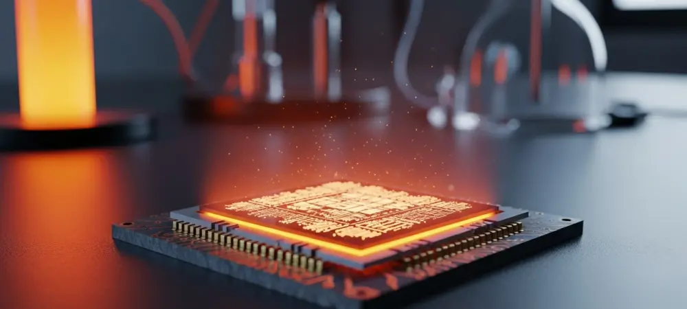
The brilliance of this design lies in its structural simplicity, though the physics behind it is incredibly sophisticated. We use tungsten on the top for its high melting point and hafnium oxide in the middle as a stable ceramic insulator, but the single atomic layer of graphene at the bottom is the real hero. Through quantum-level simulations and advanced microscopy, we discovered that graphene’s unique chemical properties prevent it from forming bonds with the tungsten. This is critical because, at extreme temperatures, metal atoms usually migrate and cause short circuits, but here, the graphene acts as an impermeable barrier that keeps the materials distinct. While this specific configuration was actually discovered by accident during experiments for a different purpose, the manufacturing involves precise layering that ensures the hafnium oxide remains an effective insulator even when the heat becomes intense enough to melt most other components.
Operating at 700°C exceeds the heat of molten lava while maintaining data for over 50 hours without refresh cycles. What were the biggest hurdles in measuring performance when the testing equipment itself was reaching its limits, and how do you validate the billion-cycle switching endurance under such stress?
Testing at 700°C creates a unique set of engineering headaches because the environment is so hostile that the laboratory equipment often fails before the chip does. We reached a point where the test equipment itself became the limiting factor, yet the device remained perfectly stable without showing any signs of degradation. To validate the billion-cycle switching endurance, we monitored the device as it operated on just 1.5 volts at nanosecond-scale speeds, ensuring that every state change was crisp and reproducible. Maintaining data for over 50 hours without a single refresh cycle at those temperatures is unheard of, especially since most electronics would have turned into a useless puddle of silicon long before that mark. It was an exercise in patience and precision, proving that the memristor could handle repeated stress that would destroy any conventional memory device.
Venusian surfaces reach 500°C, rendering most onboard computing impossible without heavy shielding. Beyond planetary probes, how would on-site computing change the safety protocols for geothermal drilling or nuclear reactor monitoring, and what are the primary trade-offs when moving away from distant, remote control systems?
Moving computing power directly to the “hot zone” changes everything for industries like geothermal energy and nuclear power where real-time data is a matter of life and death. Currently, these operations often rely on distant, remote control systems because the sensors near the heat source cannot process data locally, leading to dangerous latency or a lack of granular detail. With chips that survive 700°C, we can implement on-site computing that monitors structural integrity and temperature fluctuations with zero delay, significantly tightening safety protocols. The primary trade-off in moving away from remote systems is the initial complexity of deploying such specialized hardware, but the benefit is a massive reduction in bulky shielding and a huge leap in the autonomy of the machinery. Imagine a probe on the surface of Venus or a drill bit miles underground that can “think” and adjust its own parameters without waiting for a signal to travel back to a cool, distant server.
Most AI computations rely heavily on matrix multiplication, which memristors execute through physical processes governed by Ohm’s Law. How does this hardware-level efficiency compare to standard GPU-based processing for large language models, and what technical milestones remain before this technology can power commercial AI hardware?
When you look at systems like ChatGPT, over 92% of the computing workload is nothing more than massive matrix multiplication, which is incredibly taxing for traditional GPUs. This memristor technology performs those exact calculations through direct physical processes governed by Ohm’s Law, making it orders of magnitude faster and significantly more energy-efficient than any standard chip. We are essentially using the laws of physics to do the math rather than forcing a digital processor to cycle through billions of logic gates. However, while we have proven the concept, the road to commercial AI hardware requires us to scale these individual memristors into massive, integrated arrays. This is the first step in a long journey, but the logic is sound: we have finally created the missing component that can handle the foundational math of AI with minimal power.
Since tungsten and hafnium oxide are already standard in semiconductor fabrication, the integration of graphene appears to be the final hurdle. What challenges do industrial manufacturers face when scaling atomic-layer graphene production, and how soon could this reach a commercial production line?
The integration of graphene is indeed the final frontier, as tungsten and hafnium oxide are already “bread and butter” materials for the semiconductor industry. The main challenge for industrial manufacturers is maintaining the integrity of a single atomic layer of graphene over large-scale wafers without defects, which is a highly delicate process. Companies like Samsung and TSMC are making significant strides in graphene production, but moving it from a controlled lab environment to a high-volume assembly line is a massive undertaking. We are currently seeing the first stages of this transition through startups like TetraMem, which are focusing on commercializing memristor-based AI hardware even for room-temperature use. While a full high-temperature production line might still be several years away, the fact that two of the three materials are already standard suggests that the timeline for commercialization is much closer than people think.
What is your forecast for high-temperature electronics?
I believe we are entering an era where the “thermal barrier” in computing will simply cease to exist, leading to a proliferation of “intelligence everywhere” across the most extreme environments on Earth and beyond. Within the next decade, we will likely see the first autonomous planetary probes landing on Venus equipped with unshielded, high-performance processors that can survive for months rather than hours. Domestically, this technology will become the standard for deep-crust geothermal exploration, allowing us to tap into clean energy sources that were previously unreachable due to sensor failure. As the manufacturing of graphene matures through industry leaders, these robust memristors will not only serve extreme niches but will also migrate into mainstream AI data centers to slash energy consumption. The leap we’ve taken from 200°C to 700°C is just the beginning; the frontier of space and the depths of our own planet are finally opening up to the digital age.