
Dominic Jainy stands at the forefront of the rapidly evolving intersection between artificial intelligence and advanced semiconductor architecture. As an expert who has navigated the complexities of machine learning and blockchain, he possesses a rare perspective on how the physical limitations of hardware dictate the future of software capabilities. With OpenAI’s recent patent filings signaling a massive shift in how silicon is structured, our discussion centers on the engineering breakthroughs necessary to fuel the next generation of massive AI models. We explore the transition from traditional metal-wire connections to sophisticated embedded logic bridges that promise to redefine the density and efficiency of high-performance computing.
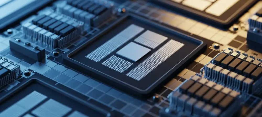
The conversation covers the transition from traditional 2.5D packaging to more flexible bridge-based designs, the significant leap in memory capacity through the integration of twenty HBM stacks, and how emerging standards like UCIe are streamlining die-to-die communication.
Standard chip designs often hit a physical wall when high-bandwidth memory must be placed within 6mm of the compute chiplet. How do embedded logic bridges extend this reach to 16mm, and what specific engineering hurdles disappear once you move beyond that traditional 6mm threshold?
The 6mm limit has long been a frustrating bottleneck for architects because it forces a cramped, claustrophobic layout where every micrometer of real estate is a battleground. By utilizing embedded logic bridges, we can effectively stretch that umbilical cord to 16mm, which provides a massive 166% increase in routing flexibility. This allows us to move away from the frantic congestion of traditional metal wires on the base layer that suffer from signal degradation over longer distances. Once you break that 6mm barrier, the nightmare of thermal management becomes much more manageable because you can physically space out the heat-generating components. It essentially opens up the floor plan of the chip, allowing for a more sophisticated arrangement of high-bandwidth memory without the constant fear of electrical interference or signal loss.
Scaling from eight memory stacks to twenty represents a massive jump in density. What are the practical implications for training much larger AI models, and how does this shift the balance between raw compute power and memory bandwidth within a single package?
Moving from the standard four, six, or eight stacks to a staggering twenty HBM stacks is like replacing a narrow suburban road with a twenty-lane superhighway. For researchers training large language models, this means a dramatic reduction in the time wasted moving data back and forth between the processor and external storage. We are seeing a fundamental shift where the sheer volume of memory on-package becomes just as critical, if not more so, than the raw teraflops of the compute engine itself. This density allows for much larger model parameters to reside directly next to the “brain” of the chip, minimizing the latency that usually kills performance in high-stakes AI workloads. It creates a more balanced ecosystem where the compute chiplet is never “starved” for data, allowing for a level of efficiency that was previously unthinkable with traditional packaging.
Embedded bridges can now double as controllers or high-speed interfaces using the Universal Chiplet Interconnect Express standard. How does integrating these functions directly into the bridge simplify the die-to-die communication, and what does this mean for the overall efficiency of high-performance computing?
By integrating the controller functionality and high-speed PHY directly into the bridge, we are essentially turning a simple “bridge” into an intelligent traffic cop that manages data flow with surgical precision. This compliance with the UCIe standard is a game-changer because it creates a universal language for different chiplets to talk to one another without needing a bulky, power-hungry translator on the main compute die. It offloads the heavy lifting of communication management, freeing up the main chiplet to focus entirely on its primary processing tasks. This streamlined die-to-die interface reduces the complexity of the internal wiring, which translates directly into lower power consumption and higher reliability for the entire system. In the world of high-performance computing, this means every watt of power is used more effectively, pushing the boundaries of what a single package can accomplish.
Emerging interconnect solutions offer a way to bypass the size limits of current base layers. If this style of advanced packaging becomes the standard for custom silicon, how would the manufacturing workflow change, and what specific cost advantages does it offer over conventional metal wire connections?
Adopting these embedded multi-interconnect bridges allows manufacturers to finally “smash” through the reticle limits of current interposers, which have historically acted as a hard ceiling on chip size. Instead of needing one massive, expensive, and fragile silicon interposer, we can use smaller, more resilient bridges to link various components together. This modular approach significantly improves yields because if one small bridge is defective, you haven’t ruined a giant, costly base layer. It’s a far more cost-effective solution than the old-school method of using dense metal wires across the entire substrate, which is both difficult to manufacture and prone to errors. We are looking at a future where custom silicon is built more like a precise assembly of high-quality blocks, reducing waste and allowing for much more ambitious designs at a lower price point.
What is your forecast for the evolution of custom AI chip architectures?
I predict that the “monolithic” era of chip design is effectively over, and we are entering a decade defined by the “Lego-ization” of high-performance silicon. We will see a massive surge in custom architectures where the compute logic is almost secondary to the sophisticated fabric of bridges and memory stacks that surround it. As OpenAI and others push for twenty or even more HBM stacks, the industry will pivot toward these embedded bridge solutions to maintain thermal and electrical integrity. Eventually, the distinction between a “processor” and “memory” will blur as these intelligent bridges take on more of the logic workload themselves. This evolution will likely lead to a new class of “super-chips” that are specifically tailored for the massive data-parallelism required by artificial general intelligence, making today’s hardware look like simple calculators in comparison.