
Dominic Jainy is a seasoned IT professional with a profound understanding of the semiconductor landscape, particularly the intricate intersection of artificial intelligence and hardware manufacturing. As the industry faces unprecedented bottlenecks in the race for AI supremacy, Dominic’s insights into the evolution of fabrication and packaging provide a crucial roadmap for understanding how global supply chains are being reshaped. From the conversion of legacy facilities to the strategic build-out of new hubs in Arizona, he offers a comprehensive look at the infrastructure fueling the next generation of high-performance computing.
The following discussion explores the logistical and strategic shifts required to solve the advanced packaging crisis, the divergence of technologies for mobile and AI applications, and the long-term implications of expanding domestic production in the United States.
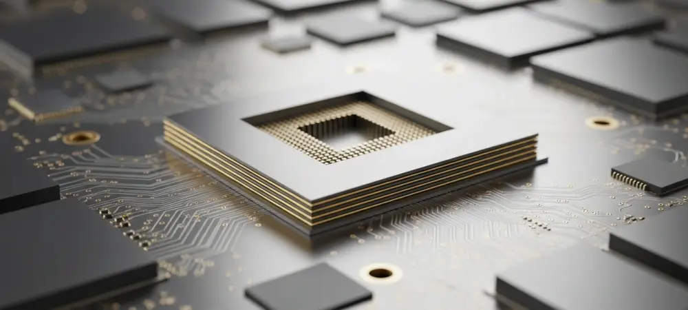
Advanced packaging has emerged as a primary bottleneck for the AI sector, leading to the conversion of older 8-inch wafer fabs into specialized packaging facilities. What are the logistical challenges of repurposing these legacy plants, and how does this shift impact the production timeline for high-performance computing chips?
Repurposing an 8-inch wafer fab is a complex undertaking because these facilities were originally designed for older, simpler processes rather than the precision required for modern 2.5D and 3D stacking. You have to overhaul the cleanroom environments and integrate entirely new specialized equipment for processes like through-silicon via (TSV) etching and micro-bumping. While this conversion saves time compared to building a “greenfield” site from scratch, it still requires a massive recalibration of the logistics chain to handle the high-value materials used in high-performance computing. By pivoting these legacy sites, we can significantly shorten the lead times for AI chips, which are currently being delayed not by the silicon itself, but by the wait for these chips to be bundled and connected in a single package.
With seven specialized facilities in Taiwan focusing on technologies like CoWoS and SoIC, the industry is racing to meet intense demand. How do these specific packaging methods differ when applied to mobile versus high-performance computing, and what steps are required to ensure these facilities reach their 2027 output targets?
The technical divergence between mobile and high-performance computing (HPC) packaging is largely a matter of scale and thermal management. Mobile packaging focuses on thinness and power efficiency, whereas HPC technologies like CoWoS (Chip on Wafer on Substrate) are designed to interconnect massive logic dies with High Bandwidth Memory, creating a large, powerful footprint that generates significant heat. To hit the 2027 targets, the industry must move beyond pilot production into a high-yield, automated environment where these seven facilities can operate in perfect synchronization. Reaching those milestones requires a relentless focus on yield rates and the steady installation of new capacity to ensure that every wafer produced actually makes it into a functional AI server.
Massive investments are being directed toward Arizona to establish domestic advanced packaging capabilities by 2030. What are the strategic implications of this geographic expansion, and how will these U.S.-based facilities address the current supply constraints that international chip fabs are facing today?
Establishing a domestic footprint in Arizona is a strategic move to close the “last mile” gap in the U.S. semiconductor supply chain, where chips were previously fabricated in the States but shipped back to Asia for final assembly. By having these two specialized facilities operational by 2030, we reduce the geographic risk and the shipping delays that currently plague international manufacturers. It creates a localized ecosystem where cutting-edge AI silicon can be designed, fabricated, and packaged all within the same region, providing a much-needed pressure valve for the global supply chain. This move isn’t just about speed; it’s about the security of knowing that the most critical components of the modern economy are not entirely dependent on a single geographic corridor.
Projections indicate that wafer output must scale from 1.3 million to 2 million units within a few years to keep pace with AI growth. What specific infrastructure or labor milestones must be met to achieve this volume, and what metrics are used to evaluate the success of such a rapid scale-up?
Scaling from 1.3 million to 2 million wafer units is a massive 54% increase in throughput that requires more than just floor space—it requires a highly skilled workforce trained in the nuances of advanced lithography and chemical mechanical polishing. We track success through “wafer-per-month” throughput and, more importantly, the final package yield, which measures how many of those complex AI packages are defect-free. To reach this volume, the infrastructure must be supported by a stable supply of high-purity chemicals and specialized substrates, which are often the hidden “choke points” in the manufacturing process. If we don’t hit the milestone of having multiple new lines certified and running at 90% plus yield by 2027, the gap between AI demand and hardware availability will only widen.
As AI packages grow larger and more complex with each generation, competitors are introducing alternative solutions like EMIB to relieve market pressure. How do these competing packaging technologies compare in terms of efficiency, and what anecdotes can you share regarding the difficulty of balancing supply and demand right now?
The competition between technologies like CoWoS and Intel’s EMIB is essentially a race to find the most efficient way to bridge the gap between processing power and memory speed. EMIB offers a high-density interconnect that can be more cost-effective for certain architectures because it doesn’t require a full silicon interposer, which is often a major cost driver. Right now, the demand is so frantic that customers are essentially knocking on every door available, willing to adapt their designs just to secure a spot on a production line. I have heard accounts of manufacturers having the actual silicon dies ready for months, but they sit idle in storage simply because there isn’t enough advanced packaging capacity to finish the product.
What is your forecast for the AI semiconductor industry’s supply chain stability?
I believe we will remain in a state of high-tension equilibrium until at least 2027, as the aggressive expansion of these seven facilities in Taiwan begins to offset the current shortages. While the transition to 2 million wafer units will provide some relief, the ever-increasing size and complexity of AI clusters mean that demand will likely stay one step ahead of capacity for the foreseeable future. However, by 2030, when the Arizona facilities come online and global capacity is more distributed, we will see a much more resilient and stable supply chain. The key will be whether the industry can maintain this “double down” investment pace without encountering a shortage of the specialized labor required to run these highly sophisticated plants.