
Introduction
The global semiconductor race has reached a fever pitch where traditional manufacturing methods no longer provide the competitive edge required to dominate the next generation of high-performance computing. Samsung is currently redefining the boundaries of fabrication by blending the analytical power of quantum mechanics with the predictive capabilities of artificial intelligence.
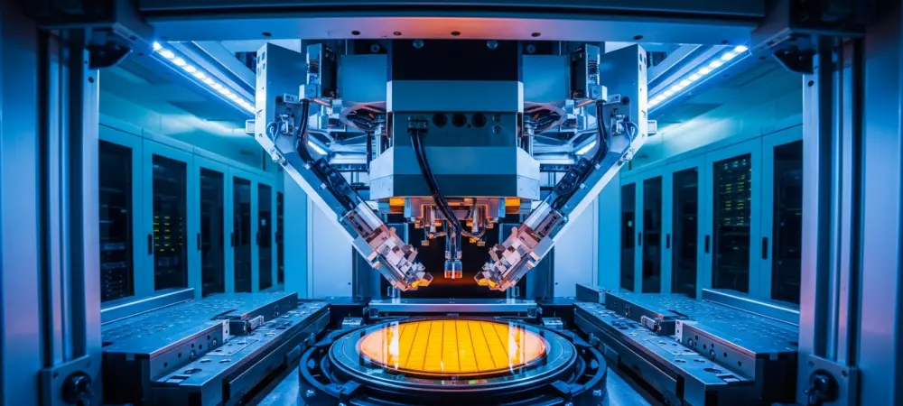
This strategic pivot targets the most complex phase of production—lithography—to ensure every silicon wafer produced meets the extreme demands of the modern hardware era. By addressing physical constraints at the atomic level, the company seeks to overhaul how chips are manufactured from the ground up to improve overall precision.
Key Questions or Key Topics Section
Why Is Samsung Prioritizing Quantum Simulations in Semiconductor Fabrication?
Lithography involves projecting circuit patterns onto silicon wafers, but as transistors shrink to smaller nodes, the margin for error becomes nonexistent. Standard computing struggles to model the complex behavior of light and chemicals at such microscopic scales, often leading to delays and wasted materials. Samsung SDS is developing quantum-powered algorithms to simulate these interactions with a level of detail that was previously impossible.
These simulations allow engineers to visualize how circuit blueprints will behave on a wafer before a single laser is fired in the cleanroom. By utilizing quantum processing, the firm can maximize transistor density and refine the etching process. This approach significantly reduces the financial resources traditionally lost to trial-and-error phases during the development of new manufacturing nodes.
How Does the Integration of Artificial Intelligence Improve the Lithography Process?
While quantum computing handles the complex physics of simulation, artificial intelligence acts as a vigilant guardian during the actual execution of the manufacturing workflow. The integration of AI allows for real-time monitoring and proactive error detection, identifying deviations in the pattern projection that human operators might overlook. This synergy ensures that the environment remains stable even under the stress of high-volume production. Moreover, the AI systems are designed to fix errors autonomously or adjust the lithography parameters toward optimal settings. By analyzing vast datasets from previous production runs, the AI refines the precision of the manufacturing nodes. This dual-layered approach not only improves the yield of functional chips but also accelerates the speed at which more powerful hardware reaches the global market.
What Are the Expected Strategic Outcomes for Samsung Electronics in the Global Market?
The primary objective behind this technological leap is to disrupt the current market hierarchy and challenge the dominance of rival firms. By securing a higher yield of premium chips, Samsung Electronics can offer more reliable supply chains to technology giants hungry for AI-capable hardware. Success in this area would translate into a significant market share increase and a stronger reputation for technical excellence. The company has already finalized the necessary algorithms and is preparing for a proof of concept next year. If the simulations prove effective, the resulting software will become a permanent fixture in their production pipeline. This evolution signifies a move away from purely hardware-based competition toward a more sophisticated, software-driven manufacturing model that leverages quantum logic.
Summary or Recap
Samsung’s focus on lithography optimization through quantum and AI highlights a path toward efficient, high-density chip production that could redefine performance standards. By prioritizing these advanced computational tools, the company is positioning itself to lead the next wave of hardware innovation. The transition to production software marks a pivotal moment for their global strategy.
This shift ensures that the manufacturing pipeline is prepared for the rigorous demands of future computing architectures. Such a move validates the role of hybrid software solutions in maintaining hardware supremacy across the global market. The integration of these technologies serves as a robust defense against the rising costs of semiconductor fabrication.
Conclusion or Final Thoughts
The shift toward quantum-enhanced manufacturing demonstrated that staying ahead in the chip market required more than just faster machines; it demanded a total rethink of simulation. Industry leaders observed how the marriage of these two technologies provided a blueprint for overcoming the stagnation of traditional silicon scaling.
These developments allowed for a more resilient production cycle that adapted to the complexities of atomic-scale fabrication. The industry reflected on this era as the point when software intelligence became the primary driver of semiconductor success.