

Introduction
The pursuit of infinite digital storage has taken a monumental stride forward as Samsung Electronics successfully unveiled its first 900-layer Vertical NAND prototype, signaling a paradigm shift in semiconductor architecture. This development is not merely an incremental update to existing flash memory; it represents a fundamental re-engineering of how memory is stacked and fused. By creating a 900-layer structure, the industry moves closer to a future where massive data centers and pocket-sized devices share the same unprecedented storage densities.
This article examines the technical innovations that made this prototype possible and addresses the competitive landscape of the memory market. Readers can expect to learn about the specific engineering techniques used to overcome physical limitations and how this breakthrough aligns with the roadmap toward 1,000-layer memory. The discussion covers everything from bonding methods to the strategic implications for the global AI hardware cycle.
Key Questions or Key Topics Section
What Technical Innovations Allow for Such High Vertical Density?
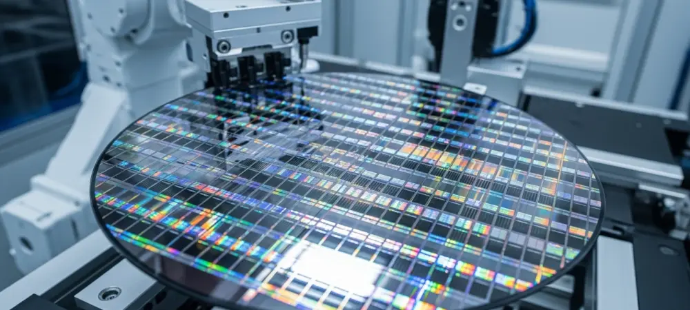
Achieving such extreme verticality requires more than just stacking layers; it demands a radical approach to wafer manufacturing. Samsung utilized a method called Cell Multi-Bonding, which essentially fuses two separate 450-layer cell wafers into one integrated unit. This technique bypasses the structural fragility that usually limits how many layers can be grown on a single substrate, allowing for a more stable and dense storage medium.
However, the physical stresses of such a design are immense, often leading to warping or misalignment that ruins the silicon. To combat these issues, engineers implemented a specialized Upper Chuck Design to stabilize the material during production. Combined with advanced Overlay Correction technology, these systems ensure that billions of microscopic connections align perfectly across the layers, maintaining the integrity of the high-capacity solid-state drives.
How Does This Advancement Impact Global Market Competition?
The semiconductor industry is currently locked in a fierce race to dominate the storage needs of the artificial intelligence era. While other manufacturers like SK Hynix have focused on the commercial release of 321-layer products, Samsung’s 900-layer prototype represents a strategic attempt to leapfrog the competition. This massive jump in density positions the company to meet the surging demands of large-scale data centers that require maximum efficiency in minimal physical space.
Meanwhile, regional players like YMTC are rapidly refining their own high-density solutions to capture a larger share of the consumer market. The arrival of a 900-layer prototype forces the entire industry to accelerate its development cycles. As a result, the transition from current standards to next-generation vertical architectures is happening much faster than analysts previously predicted, turning theoretical engineering concepts into tangible hardware realities.
Summary or Recap
The development of the 900-layer V-NAND prototype marks a turning point for memory technology, proving that the thousand-layer threshold is within reach. By successfully addressing mechanical challenges like wafer warping, Samsung has paved the way for mass-produced SSDs with unprecedented capacity. This breakthrough ensures that the infrastructure for AI and high-performance computing can continue to expand without being throttled by storage limitations.
Conclusion or Final Thoughts
The focus shifted toward how these high-density chips would eventually integrate with emerging materials like ferroelectrics to further enhance energy efficiency. Industry leaders recognized that scaling alone was no longer sufficient; the next phase of development required a holistic approach to thermal management and material science. This achievement offered a clear roadmap for organizations to begin planning for a future where storage constraints no longer dictated the limits of software innovation.