

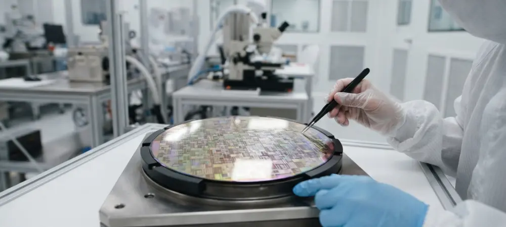
The race for semiconductor supremacy has reached a critical juncture where the physical limits of silicon are being tested by the relentless demands of artificial intelligence. As mobile devices evolve into portable supercomputers, the ability to pack more transistors into a smaller footprint has become the ultimate differentiator for global manufacturers. Samsung is currently navigating this transformation by aggressively pushing the boundaries of lithography, aiming to reclaim its position as the premier destination for high-performance computing.
The semiconductor landscape is witnessing a transition that prioritizes extreme efficiency and thermal management above all else. This shift is not merely about staying relevant; it is about defining the technical standards that will govern mobile hardware for the remainder of the decade. By focusing on the integration of cutting-edge memory and logic, Samsung aims to provide a comprehensive ecosystem that satisfies the world’s most demanding chip designers.
The High-Stakes Leap to 2nm Manufacturing
A single nanometer can determine the winner of a billion-dollar market, and Samsung is currently betting its future on the transition from 4nm to 2nm lithography. For the first time, the tech giant is moving its M2800 5G modem directly to this cutting-edge node, signaling a shift from incremental updates to a massive technological leap. This move is not merely an internal upgrade; it is a calculated strike at the heart of the global foundry market, designed to prove that Samsung can outpace the industry’s current gold standard.
The engineering required for such a jump involves overcoming immense physical hurdles related to electron leakage and heat dissipation. By bypassing the traditional intermediate steps, Samsung is positioning itself as a pioneer capable of handling the most complex fabrication tasks. This bold approach serves as a clear signal to the market that the company is ready to support the next generation of high-bandwidth communication and intensive processing tasks.
Why the 2nm Migration Dictates the Future of Mobile Hardware
The semiconductor industry is hitting a performance ceiling where traditional nodes can no longer meet the power and thermal demands of next-generation AI and 5G applications. Samsung’s success in this 2nm transition is critical because it represents the first real opportunity to break the current foundry monopoly, ensuring competitive pricing for the entire mobile ecosystem.
Beyond cost, the 2nm node is essential for the longevity of mobile devices that increasingly rely on localized machine learning. Without the efficiency gains provided by this migration, the battery life and thermal stability of future flagship smartphones would likely stagnate. Samsung is addressing these concerns by providing a roadmap that promises a significant reduction in power consumption while simultaneously increasing the raw throughput required for real-time data processing.
Synergy Between Memory and Logic: The Catalyst for Innovation
Samsung’s unique position as both a memory leader and a logic foundry is the engine behind this strategic shift. By reallocating its resources, the company is creating a ripple effect across its product lines. Utilizing the 4nm node for High Bandwidth Memory (HBM) base dies provides a significant performance advantage over the 12nm alternatives typically utilized by competitors. This approach allows Samsung to provide an integrated solution that optimizes the connection between data storage and processing.
Freeing up technical capacity has allowed Samsung to focus its most advanced engineering talent on the 2nm M2800 5G modem. The simultaneous development of 2nm flagship SoCs and modems, such as the Exynos 2700 influence, creates the technical maturity needed to stabilize the production line. This synergy disrupts the traditional foundry hierarchy by using superior HBM technology as a gateway for Samsung to secure more complex logic chip contracts from international partners.
Expert Analysis: Can Samsung Lure Qualcomm Back?
Industry analysts suggest that the maturation of Samsung’s 2nm process could fundamentally change the relationship between the world’s largest fabless chipmakers and their manufacturers. If Samsung can achieve stable 2nm yields, it can offer a performance-per-dollar ratio that the competition currently cannot match.
The prospect of a dual-foundry strategy has become an increasingly attractive option for chip designers looking to mitigate supply chain risks. Expert insights indicate that Qualcomm might adopt such a split-sourcing model to reduce the production costs of future Snapdragon chips while maintaining high performance. By proving that its 2nm line is ready for mass production, Samsung creates the leverage necessary to bring major fabless clients back into its ecosystem, potentially rebalancing market share.
Strategies for a Shifting Semiconductor Landscape
To secure this lead, Samsung prioritized the optimization of thermal management within its 5G modems to showcase the tangible benefits of the 2nm process over previous generations. The company leveraged its internal Galaxy ecosystem to achieve immediate economies of scale, which allowed it to offer aggressive pricing models that undercut the standard market rates.