
Introduction to SK Hynix’s Latest Innovation
Imagine a world where data centers powering artificial intelligence applications struggle to keep up with skyrocketing storage demands, and consumer devices crave ever-higher capacities without sacrificing speed. This is the reality of modern computing, and SK Hynix has stepped up to address these challenges with its groundbreaking 321-layer QLC NAND Flash. The purpose of this review is to meticulously evaluate whether this cutting-edge storage solution, boasting a massive 2 terabit (Tb) capacity, represents a worthwhile investment for both individual consumers and large-scale businesses.
This analysis focuses on how the technology tackles pressing storage issues, particularly in environments driven by AI and high-capacity needs. By delving into its innovative features and real-world performance, this review aims to provide clarity on its potential to transform various sectors. Readers can expect a comprehensive breakdown of its capabilities and market impact, setting the stage for an informed decision-making process.
Overview of the 321-Layer QLC NAND Technology
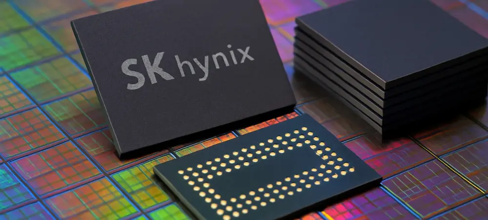
At the heart of SK Hynix’s latest offering lies the 321-layer QLC NAND Flash, a pioneering achievement as the world’s first NAND technology to surpass 300 layers using Quad-Level Cell (QLC) architecture. This remarkable feat translates into an unprecedented 2Tb capacity, catering to the insatiable demand for high-density storage. The product leverages proprietary 32DP technology, enabling the stacking of 32 NAND dies in a single package, a design that significantly enhances integration density.
Beyond sheer capacity, the technology incorporates advanced features such as an increase from four to six planes within each chip. This adjustment allows for greater parallel processing, ensuring that performance keeps pace with the massive storage potential. Such innovations make this NAND flash a versatile solution for a range of applications, from PC solid-state drives (SSDs) to enterprise SSDs (eSSDs) for data centers and Universal Flash Storage (UFS) for smartphones.
The intended use cases highlight its alignment with modern technological trends, particularly in sectors requiring robust storage solutions. Data centers supporting AI servers, for instance, stand to benefit immensely from this high-capacity offering. As industries push toward greater efficiency and scalability, SK Hynix positions this product as a cornerstone for meeting those evolving demands.
Performance Analysis of the 321-Layer NAND
When it comes to performance, the SK Hynix 321-layer NAND delivers impressive metrics that set it apart from previous generations. Data transfer speeds have been doubled, providing a substantial leap in efficiency for tasks requiring rapid access to large datasets. Additionally, write performance sees a remarkable 56% improvement, while read performance gains an 18% boost, ensuring quicker operations across various platforms.
Power efficiency also receives a significant upgrade, with write power efficiency improved by over 23%. This enhancement is particularly critical for AI data centers, where energy consumption often poses a major operational cost. The ability to process data faster while using less power translates into tangible benefits for large-scale computing environments, reducing overhead and enhancing sustainability.
These performance gains have far-reaching implications for diverse use cases. For enterprise solutions, faster data processing means improved responsiveness in critical applications, while consumer devices like smartphones can handle larger files with ease. The combination of speed and efficiency underscores the technology’s potential to redefine expectations in high-performance computing, making it a compelling choice for forward-thinking organizations.
Strengths and Weaknesses of the Technology
One of the standout advantages of the 321-layer NAND is its unparalleled storage density, a feature that directly addresses the needs of data-intensive applications. This high capacity, paired with significant performance boosts, positions it as an ideal solution for AI servers and other environments where massive datasets are the norm. The enhanced power efficiency further adds to its appeal, offering a cost-effective option for businesses prioritizing sustainability.
However, potential challenges must also be considered when evaluating this technology. Integrating such high-density storage into existing systems may pose compatibility issues or require substantial infrastructure upgrades, especially for older setups. Compared to other NAND technologies, certain niche applications might reveal limitations, such as specific performance trade-offs that could affect specialized use cases.
Balancing these strengths and weaknesses provides a clearer picture of the technology’s suitability across markets. For consumer PC users, the benefits of increased storage and speed are undeniable, while enterprises must weigh integration challenges against long-term gains. This nuanced perspective ensures that potential adopters can make decisions aligned with their unique operational needs.
Final Assessment and Recommendation
The evaluation of SK Hynix’s 321-layer QLC NAND reveals a product that pushes the boundaries of storage technology with its innovative 2Tb capacity and substantial performance enhancements. Key improvements in data transfer speeds, read and write performance, and power efficiency make it a standout option in the competitive semiconductor market. Its strategic positioning aligns seamlessly with current industry trends, particularly the growth of AI and data center demands. Based on this comprehensive analysis, a strong recommendation emerges for investing in this technology, especially for sectors poised to leverage its high-density capabilities. Businesses focused on AI-driven solutions and data-intensive operations will find it particularly valuable, as will consumer markets seeking cutting-edge storage for personal devices. SK Hynix’s vision to lead as a full-stack AI memory provider is evident in this product, which has the potential to set new benchmarks for the industry.
The company’s commitment to addressing modern storage challenges through such advancements cements its role as a market leader. For those considering adoption, the alignment with emerging technological needs makes this NAND flash a forward-looking choice. Its capacity to redefine storage standards underscores its worth as a transformative investment.
Closing Thoughts and Practical Advice
Reflecting on the overall value of SK Hynix’s 321-layer QLC NAND Flash, it became clear during this review that its transformative potential in storage technology was unmatched. The strides made in capacity and efficiency had positioned it as a game-changer for multiple industries. This innovation had not only met current demands but also anticipated future needs in an increasingly data-driven landscape.
For potential adopters, identifying the ideal user base proved essential—data center operators, tech enthusiasts, and smartphone manufacturers stood out as primary beneficiaries. Practical considerations, such as ensuring system compatibility and evaluating cost implications, were critical steps before implementation. Businesses and individuals were advised to assess how this technology could integrate into their existing frameworks without disrupting operations.
Looking ahead, the focus shifted to exploring how this NAND flash could evolve with emerging trends, such as even denser storage solutions or broader application scopes. Adopters were encouraged to balance the benefits of cutting-edge density and efficiency against specific budgetary and technical constraints. Staying informed about SK Hynix’s ongoing developments offered a pathway to maximizing the long-term value of this remarkable storage solution.