

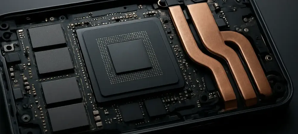
The introduction of the A20 Pro chip has fundamentally redefined the limits of handheld computing by integrating the first 2nm fabrication process into a commercially available smartphone. This technological milestone marks a clean break from the aging 3nm standards, providing the necessary architectural overhead for a sophisticated six-core CPU and a powerhouse seven-core GPU. Accompanying these core components is a specialized Dual 16-core Neural Engine that effectively reshapes how machine learning tasks are handled within a mobile chassis. Users are currently witnessing a staggering 50% increase in memory bandwidth alongside a 40% improvement in raw graphics output compared to the hardware seen in previous iterations. This level of power is not just about benchmark scores; it is about providing a silicon foundation that can sustain the intensive demands of modern software. The transition to a 2nm node allows for higher transistor density, which translates directly into better power efficiency and lower heat generation per cycle.
Advancing Artificial Intelligence and Media Processing
The evolution of the A20 Pro revolves heavily around its capacity to manage artificial intelligence and high-intensity media workflows with unprecedented speed. By doubling the AI processing capabilities of its predecessor, the chip enables features that were once considered computationally prohibitive for a smartphone. High-end photography now benefits from near-instantaneous image processing, allowing for complex multi-frame exposures and semantic segmentation without any perceptible shutter lag. Video editing enthusiasts find that the chip handles 8K resolution streams with multiple color correction layers as effortlessly as a desktop workstation. This shift is particularly visible in the responsive nature of the user interface, where predictive algorithms anticipate navigation patterns to pre-load assets. These advancements represent more than just a speed boost; they signify a move toward a truly intelligent device that learns from human behavior through consistent hardware interaction.
Moving beyond simple speed, the A20 Pro facilitates a fundamental shift by moving computationally heavy workloads away from external servers and onto the device itself. This “on-device first” philosophy ensures that sensitive user data remains private while reducing the latency associated with cloud-based processing. Sophisticated generative AI models that previously required an active internet connection to function now operate locally, providing immediate responses for text generation, image synthesis, and real-time voice translation. This architectural decision alleviates the burden on network infrastructure and allows for a seamless experience even in areas with poor connectivity. As the industry moves toward more complex digital assistants and autonomous features, having the horsepower to process these requests locally becomes a non-negotiable requirement for high-end mobile devices. The chip acts as a secure vault for private data while maintaining peak performance in all environments.
Architectural Innovations: Thermal Stability and Next Steps
A significant departure from traditional semiconductor design is found in the way the A20 Pro handles its memory and heat dissipation through a new layout. Engineers have moved away from the standard InFO POP stacked DRAM design in favor of a side-by-side configuration known as Wafer-level Multi-Chip Module (WMCM). This layout is heavily inspired by high-performance chips utilized in desktop computers, allowing for a thinner profile while maximizing surface area. By placing the memory components alongside the silicon instead of stacking them, the design eliminates the heat trap that often occurred between layers in previous chip generations. This lateral spacing allows for more efficient thermal pathways, ensuring that both the CPU and GPU can operate at their maximum clock speeds for extended periods. It is a critical change that prioritizes long-term stability over temporary peak performance bursts that cannot be sustained effectively.
Stakeholders in the mobile industry prioritized the integration of localized AI and advanced thermal architecture to secure a competitive edge during this transition. Developers optimized their software to take full advantage of the dual-core neural engines, ensuring that applications remained responsive under heavy processing loads. Manufacturers invested heavily in vapor chamber technology and WMCM packaging to prevent the performance bottlenecks that previously plagued high-end devices. This shift encouraged a broader adoption of 2nm standards across the market, pushing the boundaries of what was possible in a portable form factor. For future hardware strategies, the industry considered how to balance these power gains with sustainable energy consumption. Engineers sought out new materials for heat dissipation while refining the software-to-silicon relationship. Ultimately, the focus remained on delivering a secure and powerful user experience through innovative hardware engineering and strategic design.