
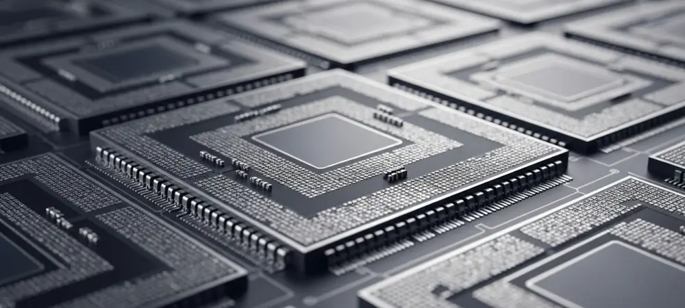
The global semiconductor landscape is currently witnessing a tectonic shift as Intel attempts to reclaim its manufacturing crown with the 14A process technology, a node that fundamentally redefines the boundaries of silicon density and architectural efficiency. This advancement represents the structural backbone of an ambition to become the world’s second-largest foundry. By focusing on a technology specifically architected for external customers, the company has pivoted toward a service-oriented model that prioritizes the requirements of the high-performance computing sector.
Strategic Evolution: Introduction to the Intel 14A Node
Intel 14A serves as a definitive answer to leading-edge offerings from global rivals. Unlike previous iterations that served internal needs, 14A is a competitive platform designed to lure tech giants through superior power-performance metrics.
This node creates a junction where manufacturing prowess meets architectural flexibility. It allows third-party designers to leverage Intel’s massive fabrication scale, signaling a departure from an historically insular production philosophy.
High-NA EUV Lithography and Transistor Scaling
Central to the 14A node is the integration of High-Numerical Aperture Extreme Ultraviolet lithography. This technology utilizes a 0.55 NA lens system, providing significantly better resolution than the standard systems used in earlier nodes.
For designers, this translates to finer circuit patterns and the elimination of complex multi-patterning. The increased precision allows for a density leap that is essential for the next generation of complex logic circuits.
Advanced Packaging and EMIB Interconnects
Complementing these advances is the Embedded Multi-die Interconnect Bridge technology. While competitors rely on 2.5D interposers, EMIB utilizes silicon bridges embedded in the substrate to connect multiple dies, offering a cost-effective solution.
This approach provides the necessary flexibility for high-performance AI accelerators. By reducing the footprint of interconnects without sacrificing bandwidth, it enables massive data throughput between compute and memory tiles in complex chiplet designs.
Recent Milestones and Development Trajectory
The transition from PDK 0.5 to the production-ready PDK 1.0 marks a vital turning point. This release provides the models and design rules that enable industry leaders to verify logic before committing to mass production.
Proactive partner engagement has streamlined the development cycle. It suggests that the technology is mature enough for high-stakes commercial silicon, moving beyond the internal focus seen in previous manufacturing roadmaps.
Real-World Applications and Industry Integration
The primary targets for the 14A node are the data centers fueling the AI revolution. Strategic partnerships with firms like NVIDIA and AMD indicate that Intel is becoming a critical infrastructure provider for advanced hardware.
Moreover, the high-performance computing sector benefits from the extreme energy efficiency that sub-2nm nodes provide. These targets reflect a consensus that Intel is making the technical strides necessary to establish itself as a primary global manufacturer.
Adoption Challenges and Market Obstacles
However, the path to dominance is fraught with technical hurdles in sub-2nm fabrication. Managing short-channel effects and maintaining consistent yields remains a significant challenge that impacts overall cost-effectiveness.
Displacing incumbents with established ecosystem loyalty requires more than technical parity. It necessitates a level of logistical reliability and cost-competitiveness that is difficult to sustain during the initial scaling phase.
Future Outlook and Infrastructure Synergy
Looking ahead, the synergy between the Ohio wafer fab and projects like the Terafab initiative points toward domestic manufacturing resilience. These projects aim to redefine the global supply chain by the decade’s end. Breakthroughs in “Terafab” scale production could potentially bypass current industry constraints. Such collaborations reflect a long-term shift toward a primary manufacturing role for the next generation of silicon.
Final Assessment of the Intel 14A Roadmap
The review demonstrated that the 14A node successfully bridged the gap between theoretical research and high-volume manufacturing. It established a new benchmark for domestic production and positioned the company as a formidable alternative.
The strategic move toward third-party integration proved effective in securing market share for the AI era. This evolution showed that strategic adjustments could redefine silicon manufacturing by creating a more diversified supply chain.