
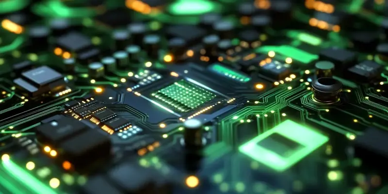
The chiplet revolution is transforming processor design, significantly impacting the future of computing. By breaking down traditional monolithic chip designs into smaller, modular components, chiplets offer increased flexibility, improved performance, and cost efficiencies. This innovative approach allows for the integration of diverse technologies within a single package, paving the way for advancements in artificial intelligence, data centers, and high-performance computing. The chiplet architecture enables manufacturers to leverage the best process nodes for different components, leading to better optimization and scalability. As the industry continues to explore the potential of chiplets, we can expect a new era of computing marked by unprecedented capabilities and efficiency.
The rapid advancement of technology has necessitated the constant evolution of computing components, particularly processors. As computational demands have grown and Moore’s Law has approached its limits, chiplet technology has emerged as a transformative solution. This article explores the evolution of chiplet technology, its manufacturing nuances, benefits, applications, and the trends shaping its adoption within the tech industry. By delving into these areas, the significance of chiplets in modern computing becomes clear, highlighting their critical role in the future of processor design and performance.
Evolution and Definition of Chiplets
Historical Context and Definition
Chiplets, which represent segmented processors rather than traditional monolithic ones, are manufactured as separate chips and subsequently integrated into a single package. Historically, this segmented design was limited to highly specialized applications, but recent technological advancements have propelled chiplets to the forefront of current technology. Today, they are integral to millions of devices, spanning desktop PCs, servers, gaming consoles, smartphones, and wearables.
The distinctive design of chiplets, contrasted with the traditional approach of using a single, unified chip, has proven advantageous in several ways. For example, it allows for a more efficient allocation of resources by dedicating different chiplets to specialized functions. This not only optimizes performance but also enhances the flexibility and scalability of processors. Furthermore, the ability to mix and match different chiplets, each manufactured using the most suitable technology for its specific function, leads to improved overall efficiency and cost-effectiveness. As a result, chiplet technology has evolved from a niche application to a mainstream solution, driving significant advancements in computing capabilities.
Transition to Mainstream Technology
The journey from monolithic processor designs to chiplet-based architectures marks a significant shift in the landscape of processor design. This evolution is primarily driven by the need for more efficient, cost-effective, and high-performance computing solutions. As the limitations of traditional monolithic chips become increasingly apparent, the industry has embraced chiplets as a viable and superior alternative. This transition was accelerated by the growing complexity of processor architecture and the rising demand for versatile and powerful computing solutions.
One of the key factors motivating this shift is the inherent flexibility of chiplet-based designs. By segmenting a processor into multiple chiplets, each tailored for specific tasks, manufacturers can achieve better performance while managing costs more effectively. Additionally, the ability to use different fabrication technologies for different chiplets means that manufacturers can optimize each part of the processor for its specific function. This not only enhances performance but also extends the practical lifespan of well-established manufacturing nodes, thereby mitigating the cost pressures associated with adopting the latest manufacturing technologies. Consequently, the transition to chiplet technology has paved the way for more innovative, efficient, and powerful processors, positioning chiplets as a cornerstone of future computing advancements.
Manufacturing and Technological Benefits
In its deliberate approach to addressing the complexities of cryptocurrencies, the SEC opted for another delay in its verdict on the spot Ethereum ETF. The extension grants the SEC an opportunity not only to conduct an in-depth examination of Ethereum’s suitability for ETF status but also to source public insight, which could heavily sway the conclusion. This speaks to the SEC’s attentiveness to the nuances of digital assets and their integration into regulatory frameworks, which it does not take lightly. The situation closely parallels the stalling faced by Grayscale, who is also waiting for the green light to transform its Ethereum Trust into a spot ETF, raising questions about the contrasting regulatory processes for Bitcoin and Ethereum.
Fabrication Process and Cost Efficiency
The manufacturing process of modern processors begins with silicon wafers, which undergo a series of complex steps involving photolithography to engrave intricate patterns. These steps culminate in the creation of individual dies that are used in processors. Amid rapid technological advancements that emphasize smaller and more efficient components, the shift to chiplets signifies a strategic pivot. By segmenting a processor into multiple dies, manufacturers can optimize each die for different fabrication technologies. This leads to significant cost efficiencies and enhanced performance.
The segmentation into chiplets allows for a more tailored and precise approach to manufacturing. For instance, high-performance logic circuits can be produced using advanced process nodes that offer superior performance characteristics, while other components like analog circuits and SRAM, which do not scale down as effectively, can utilize older, more cost-effective technologies. This strategic diversification in the manufacturing process not only reduces overall production costs but also enhances the yield of usable dies. Consequently, this results in fewer defects relative to the wafer size and contributes to more efficient utilization of resources. The net effect is a reduction in production costs and an improvement in performance, making chiplet technology a compelling choice for future processor designs.
Performance Optimization and Technological Advancements
One of the most significant advantages of chiplet technology lies in its potential for performance optimization. By separating different components into individual dies, manufacturers can leverage the most appropriate technology for each specific part. For instance, logic circuits can continue to benefit from advancements in process nodes, which are continually shrinking and becoming more efficient. In contrast, components such as analog circuits and SRAM, which do not scale down as effectively, can be manufactured using older, more stable nodes. This strategic use of different technologies ensures that each component operates at its optimal performance level.
This approach not only enhances the overall efficiency of the processor but also allows for greater flexibility in design. Manufacturers can mix and match different chiplets, each optimized for its specific function, to create processors that are tailored to the needs of various applications. This modular design also facilitates easier upgrades and improvements, as individual chiplets can be replaced or upgraded without redesigning the entire processor. Furthermore, the ability to use different technologies for different components helps to extend the practical lifespan of existing manufacturing nodes. This mitigates the challenges and costs associated with transitioning to new process technologies, thereby ensuring a more sustainable and cost-effective approach to processor design and manufacturing. Ultimately, the performance optimization and technological advancements enabled by chiplet technology represent a significant leap forward in the evolution of computing.
Case Studies: AMD, Intel, and Others
AMD’s Foray into Chiplets
AMD’s approach to chiplet technology exemplifies its power and potential. By adopting a multi-chip module (MCM) method, AMD significantly improved die yields and lowered production costs, setting a benchmark for the industry. A prime example of this evolutionary leap is seen in the transition from the single-die Ryzen 2600 to the chiplet-based Ryzen 3600. This shift epitomizes substantial improvements in efficiency and capability, showcasing the transformative impact of chiplets on modern processor design.
The pivotal point in AMD’s adoption of chiplet technology was the introduction of the Zen architecture. While Zen+ featured monolithic designs, Zen 2 embraced chiplets, strategically placing core logic and SRAM into compact dies manufactured on advanced nodes. Analog sections, on the other hand, were produced on older and cheaper nodes. This strategic reallocation allowed AMD to double the core count on desktop PCs efficiently and cost-effectively, without significantly increasing production expenses. By optimizing the use of different fabrication technologies for specific components, AMD was able to achieve remarkable performance gains and cost efficiencies, illustrating the profound benefits of the chiplet approach.
Zen Architecture and Strategic Reallocation
The Zen architecture marked a paradigm shift for AMD, introducing the concept of chiplets in a mainstream context. Zen+ represented a transitional phase with monolithic designs, while Zen 2 fully embraced the chiplet approach. In this architecture, core logic and SRAM were integrated into compact dies using cutting-edge fabrication technologies, ensuring high performance and efficiency. Analog sections, which benefit less from advanced process nodes, were produced on older, more cost-effective technologies. This strategic allocation enabled AMD to maximize performance while maintaining cost efficiency.
One of the most significant outcomes of this strategic reallocation was the ability to double the core count on desktop PCs without escalating production costs. By leveraging the benefits of advanced nodes for performance-critical components and using established technologies for others, AMD was able to deliver superior computing power at a competitive price. This approach not only underscored the flexibility and efficiency of chiplet technology but also set a new standard in processor design. The success of the Zen architecture demonstrated the potential of chiplets to revolutionize computing, providing a blueprint for future advancements in processor technology.
Intel’s Unique Approach
Intel, although later to adopt chiplet technology compared to AMD, has developed a distinctive methodology with its Meteor Lake architecture. This design divides traditional CPU components into four distinct tiles: compute, graphics, SoC, and IO. These tiles are connected via an interposer that consolidates power delivery and communication paths. This innovative approach provides Intel with greater flexibility in creating specific processors tailored for various market segments and applications.
The Meteor Lake architecture represents a significant departure from traditional monolithic designs, highlighting the evolving landscape of processor technology. By segmenting the CPU into distinct tiles, Intel can optimize each component for its specific function, resulting in improved performance and efficiency. The interposer serves as a critical element, ensuring seamless communication and power distribution among the different tiles. This modular approach not only enhances the versatility of the processor but also enables Intel to address diverse market needs more effectively. However, it also introduces complexity and cost implications, necessitating advanced manufacturing techniques and precise engineering.
Flexibility and Complexity in Design
Intel’s modular design approach, while offering significant advantages in terms of flexibility and customization, also comes with its own set of challenges. The process of integrating multiple tiles requires sophisticated manufacturing techniques and precise engineering to ensure seamless operation. Each tile must perform optimally, and the interposer must provide efficient communication and power distribution without introducing latency or other performance issues. This complexity adds to the manufacturing costs and demands a high level of precision and control.
Despite these challenges, the flexibility offered by Intel’s design is a compelling advantage. The ability to create tailored solutions for different market segments allows Intel to address specific performance requirements and optimize processor designs for a wide range of applications. This modular approach also facilitates easier upgrades and enhancements, as individual tiles can be replaced or improved without redesigning the entire processor. Overall, Intel’s unique approach to chiplet technology underscores the potential of modular designs to drive innovation and efficiency in processor technology, albeit with notable complexities that must be managed effectively.
Exploration in GPUs
The GPU sector presents another intriguing deployment of chiplet technology, particularly as computational demands in graphics-intensive applications continue to rise. AMD, leveraging its extensive experience with chiplets in CPU design, introduced multi-die designs in its Radeon 7000 series, notably in the Radeon RX 7900 GPUs. This innovative approach separates core logic from the burgeoning cache, effectively managing costs and enhancing performance without relying solely on cutting-edge fabrication nodes.
The decision to implement a multi-die design in GPUs underscores AMD’s commitment to pushing the boundaries of performance and efficiency. By isolating different functional components into separate dies, AMD can optimize each for its specific role. This separation allows for a more efficient use of resources and enhances overall performance, addressing the growing complexity and demands of modern graphics processing. Additionally, the ability to utilize various fabrication nodes for different dies helps manage production costs, making high-performance GPUs more accessible to a broader range of users. This strategy not only highlights the versatility of chiplet technology but also demonstrates its potential to drive significant advancements in the GPU market.
Nvidia and Intel’s GPU Strategies
In the realm of GPUs, Nvidia and Intel have traditionally adhered to monolithic designs, but there is increasing evidence of research and development in chiplet architecture, particularly for data center applications. Nvidia’s Blackwell GPUs, for instance, showcase high-speed chiplet designs interconnected to deliver superior performance. This approach indicates a potential shift towards chiplets in future GPU designs, driven by the need for enhanced scalability and efficiency in handling complex computational tasks.
Despite the current prevalence of monolithic GPU designs, the exploration of chiplet technology by leading companies like Nvidia and Intel suggests a forthcoming transformation in the industry. The adoption of chiplet architectures offers several benefits, including improved performance scalability, better resource allocation, and the flexibility to integrate diverse functional components. For data center applications, which demand high computational power and efficiency, chiplet designs provide a promising solution. As research and development efforts continue, it is likely that GPU manufacturers will increasingly embrace chiplet technology, paving the way for the next generation of high-performance graphics processors tailored to meet the evolving demands of advanced computing applications.
Industry Trends and Overarching Viewpoints
Physical Limitations and Moore’s Law
As chip components shrink, they inevitably encounter physical limitations that challenge traditional scaling methods. For decades, Moore’s Law has predicted the exponential enhancement of semiconductor density, driving technological advancements and the proliferation of ever-smaller, more powerful processors. However, as we approach the fundamental limits of silicon-based technology, diminishing returns are becoming increasingly apparent. This has prompted the search for innovative solutions to continue the trajectory of performance improvements without relying solely on further miniaturization.
Chiplet technology emerges as a pivotal response to these challenges, offering a new paradigm for processor design and manufacturing. By partitioning processors into smaller, specialized chiplets, manufacturers can bypass some of the limitations associated with traditional scaling. This approach enables finer control over individual components and allows for the integration of diverse technologies within a single package. The result is a more efficient, flexible, and scalable solution that extends the practical lifespan of existing fabrication methodologies. In this context, chiplet technology represents a significant shift in the industry, moving beyond the constraints of Moore’s Law and opening new avenues for innovation and performance enhancement.
Adoption by Major Corporations
Major corporations like AMD and Intel are at the forefront of this evolution, reconfiguring their manufacturing workflows to accommodate the modular approach of chiplet technology. Their adoption and investment in chiplet architecture underscore its potential to deliver cost reductions, enhanced performance, and extended technological relevance. By embracing chiplet technology, these industry leaders are setting the stage for a broader trend toward modularity in processor design, fostering a competitive environment that drives continual innovation and improvement.
The commitment of leading tech companies to chiplet technology signifies a broader industry momentum that is reshaping the landscape of processor design. AMD’s pioneering work with chiplets in its Zen architecture and Intel’s distinctive tile-based approach in the Meteor Lake architecture exemplify the diverse strategies being employed to harness the benefits of modular design. This trend is not limited to CPUs; it extends to other areas such as GPUs, where the potential for performance gains and cost efficiencies is equally compelling. As more companies adopt and refine chiplet technology, we can expect to see continued advancements that enhance computing capabilities and drive the future of high-performance processors.
Key Points and Findings
Cost Efficiency and Performance
One of the most compelling advantages of chiplet technology is its ability to reduce production costs while simultaneously enhancing performance. By segmenting chips according to their manufacturing node suitability, chiplet technology increases wafer yields, resulting in fewer defects relative to size. This approach optimizes the use of performance-specific areas such as logic or memory, ensuring that each component operates at its highest potential. The segmentation of chips into specialized dies allows manufacturers to use the most cost-effective and efficient processes for each part, further driving down production costs and enhancing overall performance.
The modular nature of chiplet technology also contributes to its cost efficiency. By using different manufacturing nodes for various components, companies can avoid the need for a single, cutting-edge fabrication process for the entire chip. This leads to significant savings in production expenses, making high-performance processors more economically viable. Additionally, the increased yield and reduced defect rates associated with chiplet-based designs contribute to more reliable and consistent performance, further solidifying the cost efficiencies offered by this approach. Overall, chiplet technology represents a strategic advancement in processor manufacturing, delivering substantial benefits in both cost and performance.
Increased Flexibility
The modular approach of chiplet technology provides unparalleled flexibility in the design and production of processors. By allowing the segmentation of chips into specialized dies, manufacturers can create tailored products that meet the specific needs of distinct market segments. This flexibility is particularly advantageous in an era of diverse computing applications, where demands for performance, power efficiency, and functionality vary widely across different devices.
For instance, high-performance servers require robust, scalable processing capabilities, while mobile devices prioritize power efficiency and compactness. Chiplet technology enables manufacturers to mix and match different chiplets to create processors that cater to these varying requirements. This adaptability extends to future upgrades and improvements as well. With a modular design, individual chiplets can be updated or replaced without overhauling the entire processor, facilitating ongoing enhancements and extending the lifespan of existing products. In essence, the increased flexibility provided by chiplet technology allows for a more responsive and dynamic approach to processor design, ensuring that advancements in computing keep pace with evolving technological and market demands.
Summary and Conclusion
In its deliberate approach to addressing the complexities of cryptocurrencies, the SEC opted for another delay in its verdict on the spot Ethereum ETF. The extension grants the SEC an opportunity not only to conduct an in-depth examination of Ethereum’s suitability for ETF status but also to source public insight, which could heavily sway the conclusion. This speaks to the SEC’s attentiveness to the nuances of digital assets and their integration into regulatory frameworks. The situation closely parallels the stalling faced by Grayscale, which is also waiting for the green light to transform its Ethereum Trust into a spot ETF, raising questions about the contrasting regulatory processes for Bitcoin and Ethereum.
The rapid pace of technological advancement has necessitated the continuous evolution of computing components, especially processors. As computational demands increase and Moore’s law nears its limits, chiplet technology has surfaced as a groundbreaking solution. This article examines the development of chiplet technology, its unique manufacturing aspects, advantages, applications, and the trends promoting its adoption in the tech industry.
Chiplet technology involves integrating multiple smaller chips, or chiplets, onto a single package, offering more flexibility and scalability than traditional monolithic designs. This approach not only helps in overcoming the limitations posed by Moore’s Law but also enhances performance and efficiency. By allowing manufacturers to use different manufacturing processes for different chiplets, this technology reduces costs and improves yields.
Chiplet technology is particularly beneficial in creating custom processors tailored to specific tasks, such as artificial intelligence, high-performance computing, and data centers. It is increasingly becoming the preferred method for developing advanced processors due to its modular nature and efficiency in handling complex computational tasks.
Innovations in interconnect technologies and packaging techniques are further driving the adoption of chiplets, promising more robust and powerful processors. As the tech industry continues to prioritize performance and efficiency, chiplet technology stands out as pivotal in shaping the future of processor design and computing performance.