
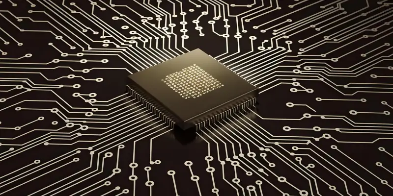
The exponential growth in artificial intelligence (AI) applications and high-performance computing has ushered in unprecedented demand for advanced semiconductor technologies. This surge necessitates a significant evolution in chip design and packaging to accommodate the computational intensity required by modern AI workloads. TSMC, a leader in semiconductor manufacturing, has announced cutting-edge innovations in chip packaging through its development of a new generation of CoWoS (Chip-on-Wafer-on-Substrate) technology. These advancements are poised to redefine benchmarks in compute performance and memory integration, addressing the intricate requirements driven by the burgeoning AI sector.
Advancements in CoWoS Technology
Scaling Multi-Chiplet Processors
TSMC’s strategic development in CoWoS technology marks a substantial leap in the realm of chip packaging. By breaking past the constraints of EUV lithography’s standard photomask reticle limits, TSMC’s CoWoS solutions currently allow interposers as large as 2,831 mm². This innovation enables the integration of multiple chiplets into a single package, supporting complex and resource-intensive AI computations. Such advancements have become crucial as AI models grow larger and require more data to process efficiently. The anticipated launch of the CoWoS-L technology is set to further push the boundaries by accommodating even larger interposers, expanding up to 4,719 mm². This increase allows for the integration of up to 12 high-bandwidth memory stacks, significantly enhancing the memory bandwidth capabilities.
The expanded interposer capacity not only facilitates more robust processing but also aligns with emerging processor designs from leading tech companies like Nvidia. The demand for enhanced processing power will see future processors like Nvidia’s Rubin GPUs achieving more than a threefold increase in compute capabilities over existing designs. As AI models become increasingly ambitious, the computational power and memory bandwidth provided by larger interposers are indispensable in delivering the necessary performance improvements. TSMC’s proactive adjustments in chip design demonstrate a thorough understanding of industry needs and position the company at the forefront of semiconductor innovation.
Power and Thermal Management
The transition toward larger chip packages and higher compute power introduces substantial challenges in power delivery and thermal management. The intensified power requirements of multi-chiplet assemblies necessitate sophisticated solutions to ensure efficient energy distribution and stability. TSMC’s advancements in this domain include the integration of cutting-edge power management circuits and monolithic power management ICs, utilizing N16 FinFET technology. By providing streamlined power routing, these developments address the considerable power demands associated with expanding processor capabilities while minimizing energy wastage.
Simultaneously, TSMC is exploring system-level co-optimization strategies to streamline power delivery and packaging with silicon design. This holistic approach allows for more efficient synchronization of components, enhancing overall system performance. Additionally, collaborative efforts with industry partners focus on developing immersive cooling solutions to manage heat output effectively. These systems are crucial for maintaining chip temperature thresholds and ensuring consistent performance. As TSMC navigates these intricate engineering challenges, its initiatives in power management and thermal regulation illustrate an acute awareness of the complexities associated with larger chip packages.
Future Trajectories in Chip Design
Expanding Performance and Integration
In the ever-evolving landscape of AI and high-performance computing, TSMC’s commitment to expanding performance and integration reaches new heights. Plans to develop an unparalleled 7,885 mm² interposer package underscore this commitment, aiming to accommodate four 3D-stacked systems-on-integrated chips and 12 HBM4 memory stacks. Such developments not only hold potential for significant performance boosts but also set new benchmarks for integration. As AI demands become increasingly intricate, these innovations offer the computational muscle necessary to power next-generation AI applications, enabling seamless processing of vast datasets.
The ambitious trajectory set by TSMC isn’t solely limited to performance. The holistic integration of various facets of chip design — from silicon architecture to packaging and power management — reflects a paradigmatic shift towards synchronizing all elements of semiconductor production. By proactively aligning these aspects, TSMC anticipates the needs of future computing environments, offering scalable solutions to meet the ever-growing demands of AI and high-performance computing. Through strategic collaborations with industry partners and investing in research and development, TSMC seeks to establish a robust foundation for continued innovation.
Challenges and Strategic Considerations
While TSMC’s innovations present promising prospects, specific challenges inherently accompany the pursuit of larger and more efficient chip designs. Power delivery, thermal management, and integration hurdles remain central issues that require ongoing attention and strategic solutions. TSMC’s investment in advanced power management techniques and immersive cooling solutions demonstrates a commitment to addressing these challenges head-on. These advancements are crucial in maintaining stability and efficiency in high-powered processing environments, essential for ensuring sustained performance.
Furthermore, the synchronization of diverse elements in chip design and operation underscores the importance of adaptability and foresight. As the computing landscape continues to evolve, TSMC’s proactive approach serves as a blueprint for successfully navigating the complexities of modern semiconductor manufacturing. Upholding a balance between innovation and practical implementation, TSMC’s efforts signify a broader industry trend towards comprehensive optimization of design, power delivery, and thermal management.
Strategic Innovations and Future Prospects
The rapid expansion of artificial intelligence (AI) applications alongside high-performance computing has sparked an unprecedented demand for advanced semiconductor technologies. This growing need mandates a significant change in chip design and packaging to support the computational power required by contemporary AI operations. Leading the charge, TSMC, a prominent player in semiconductor manufacturing, has unveiled groundbreaking innovations in chip packaging through its next generation of CoWoS (Chip-on-Wafer-on-Substrate) technology. These advancements are set to establish new standards in computing performance and memory integration, effectively addressing the complex demands brought forth by the proliferating AI sector. By significantly enhancing capabilities in these areas, TSMC’s pioneering efforts promise to revolutionize how chipsets cater to the increasing requirements of AI-driven applications, effectively reshaping the landscape of semiconductor technology for future advancements.