
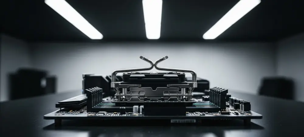
The persistent challenge of managing thermal output in modern high-performance processors has driven hardware engineers to reconsider the fundamental mechanical design of the central processing unit socket itself. As chip densities continue to climb, the structural integrity of the integrated heat spreader becomes a critical factor in maintaining consistent cooling performance across the entire surface area of the silicon. Intel is addressing this specific vulnerability with the introduction of a 2-Lever Independent Loading Mechanism for its upcoming Nova Lake processor family. By moving away from the single-lever engagement used in standard consumer hardware, this new LGA1851 implementation aims to eliminate the slight bowing that occurs when a processor is clamped into a motherboard. This curvature, while often invisible to the naked eye, creates microscopic gaps that hinder heat transfer. This shift toward a more balanced mounting force signifies a transition where mechanical precision is as vital as silicon architecture for performance.
Evolution of Thermal Interface Engineering
The development of the dual-lever system represents a refined iteration of recent experiments in socket design, specifically building upon the foundations laid during the Arrow Lake era. During that period, the industry saw the introduction of Reduced Load Independent Loading Mechanisms which managed to lower operating temperatures by a few degrees through optimized tension. However, the dual-lever approach draws deeper inspiration from legacy enterprise-grade hardware, such as the LGA-2011 sockets once found in high-end workstations and servers. Unlike standard mechanisms that push down from a single point of contact, the dual-lever system distributes clamping pressure evenly along the horizontal axis of the processor package. This design choice effectively mirrors the functionality of aftermarket contact frames. By integrating this professional-grade feature directly into the socket, the hardware provides a more stable platform for heat dissipation and maximizes cooling surface efficiency.
Strategic Implementation and Practical Outcomes
Market analysis indicated that this premium mounting solution was initially reserved for enthusiast-tier motherboards, targeting users who operated hardware at the absolute edge of thermal limits. The transition to this robust mechanical interface provided a more reliable baseline for system builders who required maximum efficiency without relying on third-party modifications. For those planning future builds, prioritizing motherboards equipped with this specific loading mechanism became a logical step to ensure long-term hardware health and sustained peak performance. Industry experts suggested that users should verify cooler compatibility with these new dimensions, as the flatter mating surface allowed for more aggressive thermal paste applications. This shift moved the focus toward holistic system design, where the socket acted as a primary thermal component rather than just a electrical bridge. The hardware community recognized that stabilizing the physical contact between the chip and the cooler remained a cost-effective way to unlock performance.