
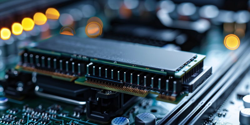
As the digital era races forward, the relentless demand for higher data rates and greater memory capacity has driven industry giants like Samsung and SK Hynix to spearhead the next leap in high bandwidth memory (HBM) technology. The HBM4 standard, anticipated to debut between 2025 and 2026, promises to redefine the landscape of high-performance computing and AI applications.
Samsung Rises to the Challenge
Embracing 1a DRAM for a Competitive Edge
Samsung’s strategic shift to 1a DRAM marks a pivotal move in the HBM4 arena. This evolution in DRAM technology, expected to hit mass production by late 2024, not only bodes a resurgence in Samsung’s competitive stance but also signifies an industry trend toward power-efficient memory solutions. With an initial production volume of 3000 units per month, Samsung aims to scale up its capacity rapidly, ensuring it remains at the forefront of the memory sector. Successful integration of 1a DRAM could well be the catalyst needed for Samsung to overcome recent challenges in qualifying tests for NVIDIA’s AI GPUs, thereby securing its position as an indispensable partner in cutting-edge memory innovation.
SK Hynix’s Pursuit of Excellence with 1a and 1b DRAM
Noting Samsung’s pivot, SK Hynix is not far behind, implementing 1a DRAM in its HBM4 offerings while simultaneously setting sights on 1b DRAM for the forthcoming HBM4E memory. This methodical approach underscores the company’s dedication to continuous innovation and the incessant quest for enhanced energy efficiency. As these titans vie for industry dominance, such advancements suggest a broader shift in the market, where sophisticated technologies not only meet the current demands but shape the future contours of the high-bandwidth memory landscape.
TSMC Joins the Fray
Paving the Way with Tailored Base Dies
TSMC casts a significant shadow in the field of memory integration, particularly with its plans to produce tailored base dies that will serve as the foundation for the new HBM4 stacks. By tapping into its advanced N5 and N6 process nodes, TSMC is addressing the complex transitional needs from the 1024-bit to the 2048-bit interfaces. This technical prowess ensures the provision of logic that is not only powerful but also power-efficient, a detail of crucial importance within the next-generation GPU accelerators primed to harness this memory revolution. TSMC’s forward-looking approach further solidifies the collective push by industry heavyweights to meet and exceed the thresholds of what is possible in memory technology.
Strategic Crafting for Future Demands
In an era where faster data transfer and large memory storage are critical, tech giants like Samsung and SK Hynix are at the forefront of the latest advancements in memory technology. With the development of High Bandwidth Memory 4 (HBM4), these companies are setting the stage for a significant evolution in the realm of high-performance computing and artificial intelligence. Expected to be unveiled between 2025 and 2026, HBM4 will offer an unprecedented increase in data rate and memory capacity, enabling more efficient and powerful computing capabilities. This innovation is essential as the world becomes increasingly reliant on complex algorithms and computing systems that demand rapid access to large volumes of data. The introduction of HBM4 technology is eagerly awaited as it is poised to revolutionize the efficiency and processing power of next-generation computers and AI systems, thus meeting the accelerating requirements of the digital age.