

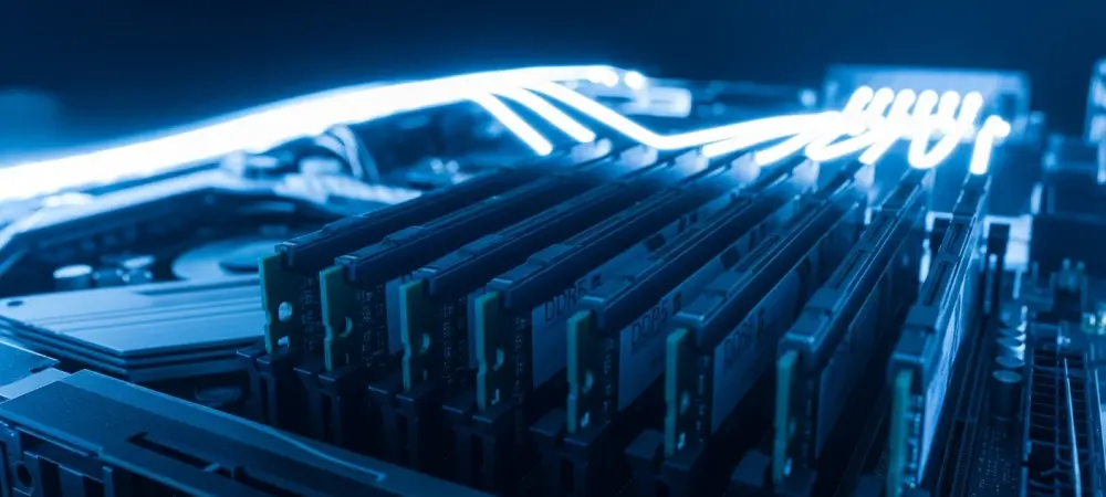
The insatiable demand for local inference capabilities in modern workstations has pushed traditional memory architectures to their absolute breaking point. This shift toward high-performance solutions is no longer optional for maintaining system integrity as generative models move from the cloud to the edge.
The transition toward the Rambus DDR5 Gen2 Client Chipset represents a pivotal moment for both hardware enthusiasts and enterprise users. It provides the necessary bandwidth to sustain the heavy data throughput required by the next generation of processors while maintaining signal stability.
Evolution of High-Speed Memory for the AI PC Era
The move toward specialized high-performance architectures is a direct response to the limitations of standard DDR5. While early iterations focused on capacity, the current landscape prioritizes throughput and latency to keep up with the rapid execution cycles of modern neural networks.
This evolution has moved the industry away from generic unbuffered modules toward sophisticated “clocked” memory form factors. By integrating advanced conditioning logic directly onto the module, the hardware can now support the extreme bandwidth required by autonomous software agents.
Core Components of the Gen2 Client Chipset
The CKD02: Gen2 Client Clock Driver
As DDR5 frequencies scale past 6400 MT/s, signal degradation becomes a primary obstacle for system designers. The CKD02 addresses this by acting as a buffer that retimes and conditions the clock signal before it reaches the DRAM components on the module.
This ensure that timing remains precise even when the processor is operating at peak loads. By stabilizing the clock at 9600 MT/s, Rambus enables a level of performance that was previously reserved for high-end servers, effectively eliminating the bottleneck between CPU and RAM.
Optimized Power Management: The PMIC5120
Power delivery is just as critical as signal timing at high frequencies. The PMIC5120 manages the voltage supply directly on the module, allowing for localized regulation that is far more efficient than traditional motherboard-level control.
This proximity reduces electrical noise and ensures that the active components receive a steady, clean power supply during rapid state transitions. Such efficiency is vital for high-performance laptops where cooling capacity is limited yet performance cannot be compromised.
The SPD Hub and Telemetry Integration
Effective memory management requires more than just raw speed; it requires intelligence. The SPD Hub serves as the module’s identification center, storing configuration data that the system uses to boot and operate correctly under varying conditions.
In the Rambus Gen2 chipset, this hub also provides real-time telemetry. This allows the system to monitor temperature and power consumption, enabling the BIOS to make dynamic adjustments that preserve hardware health while maximizing performance during intensive workloads.
Emerging Trends in Clocked Memory Architectures
The industry is currently moving toward a standard where every high-performance DIMM includes a clock driver. This trend is visible in the emergence of CUDIMM and CSODIMM formats, which are specifically designed to handle the rigors of speeds exceeding 9000 MT/s. Hardware designers are now treating memory modules as active components with their own internal processing and regulation logic to bypass the physical limitations of traditional traces.
Real-World Applications in Next-Generation Computing
The most immediate impact of this chipset will be seen in platforms like Intel’s Nova Lake and AMD’s Zen 6 architectures. These processors are designed to leverage the 9600 MT/s ceiling to significantly improve the performance of integrated AI accelerators and graphics units.
For professionals working in scientific simulation or video production, this means faster data processing and reduced render times. In the mobile space, it allows workstations to maintain desktop-class performance, which is essential for developers training large models locally.
Technical Hurdles and Industry Adoption Barriers
Transitioning to these extreme frequencies is not without challenges. Signal degradation and thermal management remain the two biggest hurdles for engineers, as the margins for error are razor-thin when data moves at such incredible speeds.
The industry must also navigate the complexity of physical standard changes and the higher cost of manufacturing sophisticated modules. Balancing the need for performance with the practicalities of mass manufacturing remains a primary focus for the semiconductor sector.
Future Outlook for DDR5 and Beyond
Looking ahead, the scaling of DDR5 is likely to push well past the 9600 MT/s mark as manufacturing processes for both DRAM and chipsets mature. This continued growth in bandwidth will be the foundation for even more capable and autonomous software environments. As software becomes more complex, the demand for memory that can provide instantaneous access to context windows will only intensify. This progress paves the way for a future where personal computers act as active participants in complex problem-solving rather than passive tools.
Final Assessment of the Rambus Client Solution
The Rambus DDR5 Gen2 Client Chipset proved to be a necessary intervention in an industry struggling with the physical limits of memory. By stabilizing speeds that were once considered impossible for client hardware, it provided the groundwork for the AI PC era to truly begin.
The technology shifted the focus from simple capacity to a more balanced approach involving intelligence and signal stability. Ultimately, this chipset enabled a new level of local computing power that redefined what was possible for both professional and creative workflows.