
Dominic Jainy is a seasoned IT professional whose expertise spans the critical intersections of artificial intelligence, machine learning, and semiconductor evolution. With a deep focus on how emerging hardware architectures drive software capabilities, he has become a key voice in analyzing the shift toward high-performance, integrated silicon solutions. As the industry moves toward “Halo-class” processors that blur the lines between mobile efficiency and desktop power, his insights provide a roadmap for the next half-decade of computing. This conversation explores the technical resurgence of on-package memory, the architectural rivalry between industry titans, and the engineering hurdles of fusing disparate silicon layers into a single, cohesive unit.
Intel is revisiting on-package memory for the upcoming Razor Lake-AX chips, potentially utilizing LPDDR6 or Z-Angle Memory. How does moving DRAM directly onto the package impact thermal management, and what specific bandwidth improvements can developers expect for high-end integrated graphics?
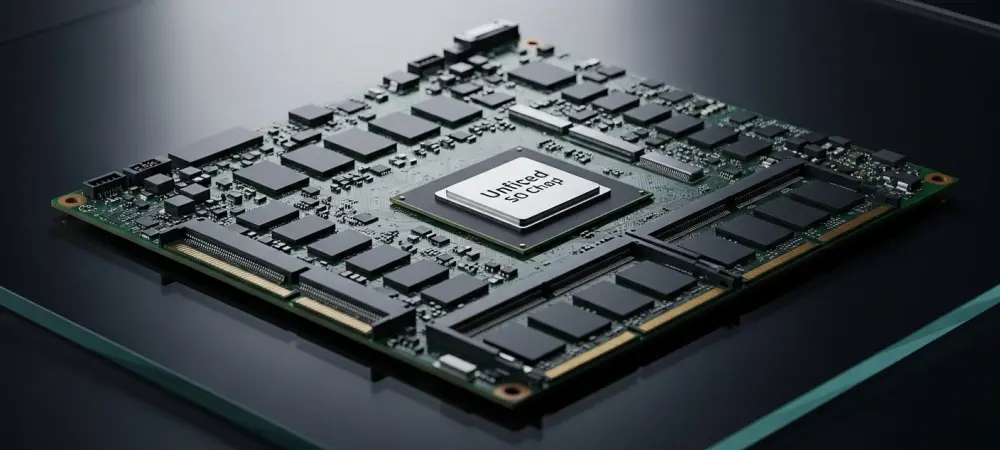
Moving DRAM directly onto the package is a double-edged sword that requires a masterclass in thermal engineering. While it significantly reduces the physical distance signals must travel—cutting down on latency and power leakage—it concentrates heat in a much smaller footprint, which is particularly challenging for a high-end chip like Razor Lake-AX. By 2028, we expect to see LPDDR6 or Intel’s own Z-Angle Memory (ZAM) providing the massive bandwidth necessary to feed a large iGPU. This transition is essential because integrated graphics are often starved for data; moving to these newer standards on-package will provide the throughput required for high-fidelity rendering without the bottleneck of traditional motherboard traces. Developers should prepare for a design environment where the distinction between “system memory” and “video memory” effectively vanishes, allowing for more fluid asset streaming in real-time applications.
The high-end mobile market is shifting toward “Halo-class” APUs, pitting Razor Lake-AX against competitors like AMD’s Medusa Halo. What architectural advantages do Griffin Cove P-Cores and Golden Eagle E-Cores provide in this matchup?
The architectural battle between Intel’s Razor Lake-AX and AMD’s Medusa Halo will be won on the efficiency of heterogeneous computing. The Griffin Cove P-Cores are being refined to handle heavy, bursty workloads with high instructions-per-clock (IPC) performance, while the Golden Eagle E-Cores manage the dense, multi-threaded background tasks. This “Halo-class” segment is unique because it demands sustained peak performance that usually requires a discrete GPU, but within a 30W to 80W envelope. In previous generations, we’ve seen that pushing high core counts in a dense SoC often leads to aggressive thermal throttling. By utilizing the 18A process node or its derivatives, Intel aims to balance these cores so that the “Golden Eagle” clusters can maintain high throughput for AI and productivity tasks without cannibalizing the power budget needed for the “Griffin Cove” cores during gaming.
Razor Lake is expected to maintain socket and pin compatibility with Nova Lake platforms for standard S, H, and HX families. How does this continuity influence long-term motherboard development, and what are the primary challenges of integrating high CPU and GPU core counts into a single SoC?
Maintaining socket and pin compatibility between Nova Lake and Razor Lake, specifically the LGA 1954 socket, is a strategic move that provides a stable four-to-five-year roadmap for motherboard manufacturers. It allows OEMs to amortize their research and development costs over multiple generations, which eventually leads to more refined power delivery systems and better signal integrity for PCIe Gen 5.0 and beyond. However, the “AX” variant is a different beast entirely because it integrates a massive GPU and embedded cache onto the same silicon as a high-performance CPU. The engineering challenge here is “die-to-die” or “tile-to-tile” interconnectivity; you have to stitch together these high-count core complexes while ensuring that the heat generated by the GPU doesn’t degrade the clock speeds of the CPU cores. This necessitates a more complex manufacturing step involving advanced packaging technologies like Foveros to stack or tile these components vertically and horizontally.
With the potential integration of Xe4 “Druid” graphics architectures by 2028, integrated performance is reaching parity with discrete GPUs. How will this evolution change the design of ultra-portable laptops, and what roles will embedded cache and advanced controllers play?
The arrival of the Xe4 “Druid” architecture within the Razor Lake-AX ecosystem marks the end of the “budget” integrated graphics era. We are moving toward a reality where an ultra-portable laptop can deliver performance that currently requires a mid-range discrete GPU, essentially making the laptop thinner by removing the need for a secondary cooling loop and dedicated VRAM chips. The embedded cache acts as a high-speed buffer that minimizes the need to access the LPDDR6 memory, which is vital for maintaining high frame rates at 1440p or 4K resolutions. Advanced controllers will play a “traffic cop” role, intelligently routing data between the CPU, the NPU for AI tasks, and the Xe4 cores to ensure that power is never wasted on idle components. This transition will be measured by a significant jump in “performance per cubic millimeter,” allowing for sleek designs that don’t compromise on professional-grade rendering or gaming capabilities.
Future custom SoCs may fuse x86 architectures with high-end NVIDIA RTX GPUs. What are the integration hurdles when combining these different silicon layers, and how will this affect the market for traditional gaming laptops?
Fusing Intel’s x86 cores with NVIDIA’s RTX GPUs in a “Serpent Lake” style SoC represents the ultimate engineering synergy, but the hurdles are massive, specifically regarding proprietary interconnects and thermal profiles. You are essentially taking two different design philosophies—Intel’s compute-centric tiles and NVIDIA’s graphics-centric architecture—and forcing them to share a single piece of silicon and a unified thermal solution. The engineering process involves creating a custom fabric that allows the RTX cores to access the system’s on-package memory with the same low latency as a dedicated GDDR6X bus. If successful, this will cannibalize the traditional entry-level and mid-range gaming laptop market, as the need for a separate GPU chip and its associated PCB space disappears. This leads to massive power efficiency gains because you eliminate the energy cost of moving data across a PCIe bus between two separate chips.
What is your forecast for the on-package memory market over the next five years?
I forecast that on-package memory will move from being a niche feature for low-power ultrabooks to the industry standard for all high-performance mobile computing by 2029. As we see with the transition from LPDDR5X to LPDDR6, the demand for bandwidth in the age of on-device AI and “Halo-class” APUs will make traditional SODIMM slots a relic for everything except specialized workstations. We will likely see a bifurcated market: desktop users will retain modularity with standard DDR5/DDR6, but the mobile and “compact PC” sectors will shift almost entirely to soldered, on-package solutions to maximize efficiency and performance. By the time Razor Lake-AX matures, the integration of memory, cache, and compute will be so tight that the very concept of a “component” will shift toward a singular, unified “compute tile.”