

The relentless pursuit of silicon supremacy has pushed semiconductor engineering to a critical threshold where traditional manufacturing physics no longer offer a clear path toward progress. The Intel 14A2 process technology represents a significant advancement in the semiconductor manufacturing sector. This review explores the evolution of the technology, its key features, performance metrics, and the impact it has on various applications.
This analysis provides a thorough understanding of the technology, its current capabilities, and its potential future development. By moving beyond the 2nm barrier, the platform addresses the cooling and power delivery bottlenecks that have plagued high-density chips. It serves as a testament to the viability of modern lithography in an increasingly demanding digital landscape.
The Strategic Emergence of the 14A2 Node
Intel’s introduction of the 14A2 process marks a critical pivot in its “IDM 2.0” strategy, aiming to reclaim silicon leadership in the sub-2nm era. Emerged as a sophisticated refinement of the foundational 14A node, this technology is designed to compete directly with TSMC’s A14 process and Samsung’s 1.4nm roadmap. By accelerating its development cadence, Intel is positioning its foundry services as a viable, high-performance alternative for external customers who have traditionally relied on Asian manufacturing hubs.
The node serves as a cornerstone for efforts to establish a dominant presence in the global foundry landscape by the end of the decade. This transition is not merely a technical upgrade but a business necessity to diversify supply chains. As global demand for high-end logic remains volatile, providing a stable, American-based manufacturing alternative has become a primary selling point for the company.
Technical Innovations and Architectural Enhancements
Dual-Side Power Delivery: Network Optimization
A primary differentiator of the 14A2 node is the transition from a standard Backside Power Delivery Network to a “Dual Side” architecture. While the initial 14A process utilizes PowerDirect technology to route power through the rear of the wafer, the 14A2 refinement integrates both front-side and back-side routing. This hybrid approach is essential for managing the extreme electrical demands of ultra-high-density transistors, ensuring that power delivery remains stable without compromising signal integrity.
Moreover, this architecture optimizes thermal performance by distributing the electrical load across a wider physical area. By separating the signal and power tiers more effectively, the design reduces the risk of electromigration. This ensures that the chip can maintain peak performance over a longer lifecycle, which is a critical requirement for enterprise-level deployments where uptime is a priority.
Transistor Density Scaling: High-NA EUV
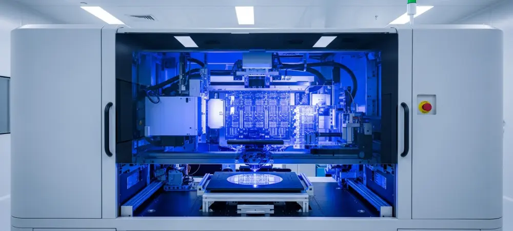
The 14A2 node pushes the boundaries of lithography by reducing the M0 pitch from 28nm to 21nm. This aggressive scaling is achieved through the integration of High-NA (Numerical Aperture) EUV equipment combined with advanced double patterning techniques. These enhancements allow for transistor density gains that significantly exceed the 30% improvement projected for the standard 14A process.
Shrinking the physical footprint of logic gates while maintaining performance provides a pathway for more complex processor designs. This precision allows for a more granular control over the etching process, reducing variability across the wafer. Consequently, the manufacturing process achieves higher consistency, which translates to better binning results and more efficient silicon utilization for high-volume production runs.
Evolution of Manufacturing Paradigms in the Sub-2nm Era
The semiconductor industry is currently witnessing a shift toward “Gen2” refinements that maximize the utility of extremely expensive fabrication equipment. The development of 14A2 reflects an industry-wide trend where manufacturers must iterate rapidly on existing nodes to justify the massive capital expenditure of High-NA EUV tools. This era is defined by a focus on “foundry-first” logic, where process predictability and yields are prioritized to attract high-profile fabless clients. Intel’s move to 14A2 illustrates a broader trend of aggressive roadmap expansion to stay ahead of the Moore’s Law curve. This strategy relies on overlapping development cycles, where research on the next node begins long before the current one reaches peak volume. This continuous iteration model ensures that the fabrication plants never sit idle, maintaining a steady flow of innovation and revenue to support future research and development.
Industrial Applications and Market Positioning
The 14A2 technology is specifically tailored for the burgeoning AI and High-Performance Computing markets. These sectors require the massive transistor counts and sophisticated power management that 14A2 offers to drive next-generation large language models and data center infrastructure. Beyond internal use, Intel is positioning 14A2 as a premium offering for external silicon designers, providing a high-capacity alternative to traditional leaders.
This positioning is vital for sectors that require sovereign manufacturing capabilities or diverse supply chain options for mission-critical hardware. Furthermore, the efficiency gains of the 14A2 node make it an attractive choice for autonomous vehicle systems. In these environments, processing power must be balanced with strict energy constraints, a challenge that this node addresses through its refined power delivery network.
Engineering Challenges and Scaling Obstacles
Scaling to a 21nm pitch introduces formidable technical hurdles, most notably increased electrical resistance and the physical limits of Nano Through Silicon Vias. As interconnects shrink, maintaining low-latency communication between layers becomes increasingly difficult. Intel’s use of composite structures—balancing power delivery between the front and back of the chip—is a direct response to these specific physical limitations. Furthermore, the market transition to such advanced nodes faces economic obstacles, as the cost per wafer for High-NA EUV manufacturing remains significantly higher than previous generations. Ensuring high yields was paramount to maintaining commercial viability for external clients. Without consistent yield rates, the price-to-performance ratio could alienate potential partners who are sensitive to the rising costs of advanced silicon fabrication.
Future Trajectory: The Path to 1.4nm Dominance
Looking ahead, the 14A2 node serves as the bridge to the long-term goal of mass-producing 1.4nm-class chips by 2029. Success in this node will likely dictate the ability to sustain the roadmap and compete with TSMC’s upcoming A14 fabs. Potential breakthroughs in materials science, such as the adoption of new conductive metals, may further enhance the performance of subsequent iterations.
The long-term impact of this technology will be felt across the entire tech stack, enabling a new generation of edge computing and autonomous systems. As devices require unprecedented levels of on-chip intelligence, the 14A2 node provides the necessary density to house complex AI accelerators alongside traditional logic. This convergence of capabilities will redefine how data is processed at the source.
Final Assessment of Intel’s 14A2 Capability
In summary, the Intel 14A2 process technology stood as a calculated and aggressive leap in semiconductor fabrication. By combining High-NA EUV lithography with a novel dual-side power delivery system, the engineering teams addressed the dual requirements of transistor density and electrical stability. The technical and economic hurdles remained substantial, yet the node’s potential to disrupt the current foundry hierarchy proved significant.
The transition required a reimagining of how silicon was powered, shifting the industry focus toward hybrid delivery models. If the manufacturing complexities of the 21nm pitch were successfully navigated, 14A2 secured a pivotal achievement in the quest to lead the sub-2nm era. Future iterations will likely build upon this foundation, incorporating new 2D materials to further reduce latency. This development cycle ultimately redefined the future of high-performance silicon and set a new standard for foundry capabilities.