
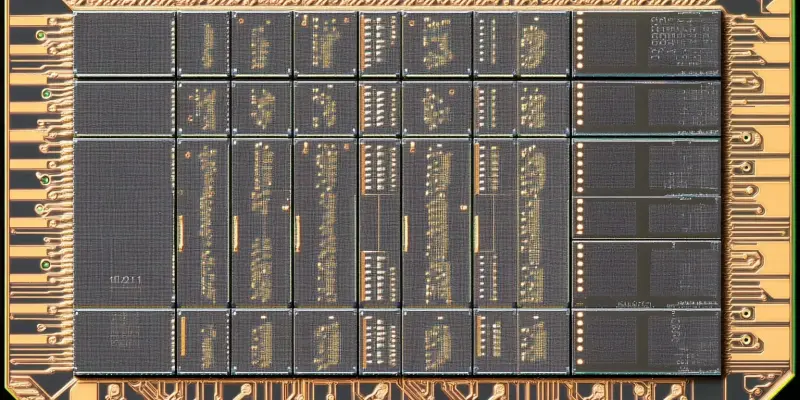
In a groundbreaking achievement that promises to reshape the memory technology landscape, SK Hynix, the world’s second-largest memory chipmaker, has successfully become the first to mass-produce triple-level cell (TLC) NAND with 321 layers. This technological feat sets the company ahead of its rival Samsung and heralds a new era in storage solutions by delivering higher-capacity memory at more affordable prices. The introduction of SK Hynix’s 1-terabit 4D NAND chips marks yet another significant milestone, especially after being the pioneering force behind the launch of 238-layer NAND less than a year ago. These advancements are expected to substantially enhance storage density for both consumer and enterprise solid-state drives (SSDs), potentially offering capacities that exceed 100TB. Such high-capacity and energy-efficient storage solutions are particularly advantageous for artificial intelligence (AI) data centers and other high-performance applications that require substantial storage capabilities.
Pioneering New Technological Heights
The breakthrough achieved by SK Hynix was made possible through their innovative “Three Plugs” technology, which optimizes the electrical linking process by connecting three memory layer vertical channels. This advanced method also incorporates the development of new low-stress materials as well as automatic alignment correction to address stress and alignment issues during manufacturing. The technological refinements have led to a significant 59% improvement in production efficiency compared to the previous generation. The new 321-layer chips boast 12% faster data transfers, 13% faster reading speeds, and offer over 10% better power efficiency than the earlier 238-layer NAND. This represents a significant leap in both performance and cost-effectiveness, illustrating how SK Hynix’s dedication to innovation continues to push the boundaries of what is possible within the field of NAND flash memory technology.
Coupled with these impressive advancements, SK Hynix has announced plans to begin shipping these new storage devices in the first half of 2025. The initial focus will be on the AI market, where the need for high-capacity, energy-efficient storage is constantly growing. Following this, applications will broaden to include ultra-high capacity SSDs for gaming, media editing, and extensive data storage requirements. These developments are set to fuel further growth and innovation within these industries, underscoring the transformative potential of SK Hynix’s cutting-edge NAND technology.
The Competitive Landscape
In light of SK Hynix’s significant milestones, competing memory chip giant Samsung is actively working on its own cutting-edge NAND technology. Samsung aims to release a 400-layer NAND by 2026 and has advanced plans for bonded vertical NAND technology. This could result in chips with over 1,000 layers and SSDs potentially exceeding 200TB by 2030. This technological race underscores the intense competition in the industry to push storage capacity and efficiency to new heights. Similarly, Japan’s Kioxia is pursuing comparable advancements, maintaining a dynamic and competitive landscape.
This burgeoning competition among leading memory chip manufacturers highlights a crucial trend toward denser and more efficient storage solutions, vital for satisfying the increasing demands of AI, gaming, and high-performance computing. As NAND flash memory technology evolves, both consumers and industries can expect unparalleled advancements in storage capabilities, fueled by relentless innovation and competition. The strides made by SK Hynix have indeed transformed the field, and their ongoing efforts are likely to spur further breakthroughs in memory technology.