
The relentless expansion of global data traffic has reached a critical juncture where current microwave-based communication systems are increasingly unable to satisfy the bandwidth requirements of the near future. As the industry transitions from the foundational successes of 5G technology into the conceptual and experimental realms of 6G, the primary objective has shifted toward achieving terabit-per-second data speeds. This monumental leap in performance is necessitated by a new generation of data-intensive applications, ranging from autonomous swarm robotics and real-time medical imaging to the creation of persistent digital twins that mirror complex physical environments. However, reaching these speeds requires a fundamental migration of carrier frequencies into the sub-terahertz (sub-THz) range, a territory where traditional semiconductor technologies often struggle with issues of efficiency, size, and signal integrity.
Current sub-THz receivers generally rely on complex architectures that incorporate high-frequency mixers, local oscillators, and heavy external focusing elements. While technologies such as Schottky barrier diodes have demonstrated impressive data rates, they frequently suffer from a lack of CMOS compatibility and high power consumption requirements. Furthermore, the physical footprint of these devices, often exacerbated by the need for bulky silicon lenses or horn antennas, makes them difficult to integrate into the compact, power-constrained environments of mobile handsets or distributed Internet of Things (IoT) sensors. The challenge, therefore, lies in finding a material platform that can offer high-speed operation and low noise while remaining scalable and easy to manufacture within existing industrial frameworks. Graphene has emerged as a uniquely qualified candidate to break this terabit barrier by unifying high-speed detection with a compact, low-power footprint. By leveraging the exceptional carrier mobility and the photothermoelectric properties of this two-dimensional material, researchers have developed a receiver architecture that operates at zero-bias, effectively eliminating dark current and significantly reducing the complexity of the accompanying electrical circuitry. This graphene-based approach provides a path toward monolithic integration with standard silicon technology, offering a versatile solution that addresses the physical and economic limitations currently hindering the widespread deployment of 6G infrastructure.
Addressing the Terabit Barrier in Next-Generation Wireless Connectivity
The demand for wireless data capacity has historically followed Edholm’s Law, which observes that data rates for both wired and wireless communication tend to double approximately every eighteen months. To maintain this trajectory through the next decade, the industry must prepare for a world where wireless links operate at speeds exceeding 100 gigabits per second, eventually scaling to a full terabit. This shift is not merely about faster downloads but is a prerequisite for the ultra-low latency required by 6G applications, such as remote surgery and complex industrial automation. In these scenarios, even a microsecond of delay can lead to catastrophic failures, making the transition to the high-bandwidth sub-terahertz bands an absolute necessity rather than a luxury.
However, the leap to these higher frequencies introduces a set of formidable engineering obstacles that current hardware is ill-equipped to handle. Most contemporary sub-THz receivers are built using electrical or optical schemes that involve significant trade-offs. Electrical systems often struggle with non-linearities and non-flat frequency responses caused by the necessary mixing stages, while optical receivers like Schottky barrier diodes often require air-bridge structures that are difficult to manufacture at scale. Furthermore, the high power consumption of these active components poses a significant barrier for mobile and battery-powered devices, which require passive or extremely low-power detection mechanisms to remain viable in the field. Graphene-based receivers offer a transformative solution by integrating high-speed operation and low-noise performance into a single, CMOS-compatible platform. Because graphene is a zero-gap semimetal with incredibly high electron mobility even at room temperature, it can respond to electromagnetic radiation across an incredibly broad spectrum. By designing devices that utilize the photothermoelectric effect, engineers can create sensors that generate a voltage directly from incident radiation without the need for an external power supply. This zero-bias operation is the key to creating the ultra-low-power, high-density receiver arrays that will be needed to blanket urban environments with 6G connectivity.
The Evolution Toward Sub-Terahertz Communication Systems
The identification of the 0.2 to 0.3 THz band as the “sweet spot” for 6G communications is the result of a careful balancing act between the need for massive bandwidth and the harsh realities of atmospheric physics. At frequencies above 1 THz, atmospheric attenuation becomes so severe that signal propagation is limited to extremely short distances, rendering it impractical for most terrestrial communication. In contrast, the 200 to 300 GHz window offers several atmospheric “transparency windows” where signal loss is manageable, yet the available bandwidth is still hundreds of times greater than what is currently used in the microwave bands. Utilizing this spectrum effectively requires a new class of receivers that can operate with high sensitivity despite the inherent losses of free-space propagation.
Existing technologies, such as plasmonic modulators and Schottky barrier diodes, have paved the way for high-speed sub-THz links, but they are often hindered by their reliance on off-chip components. For example, many high-performance detectors require hemispherical silicon lenses to focus the broad THz beam onto a tiny active area. These lenses not only increase the cost and complexity of the receiver but also prevent the kind of dense, on-chip integration required for modern electronics. Furthermore, many of these systems involve high-speed electrical mixers that are difficult to tune and generate significant heat, which is a major drawback for the compact hardware envisioned for the 6G era.
The pursuit of an integrated, passive, and scalable technology has led researchers to look toward two-dimensional materials as the foundation for the next generation of wireless infrastructure. A successful 6G receiver must be able to convert sub-THz radiation directly into an electrical signal that can be processed by standard 50-ohm electronics without the need for additional upconversion or complex matching networks. By focusing on graphene, which can be grown at a large scale using chemical vapor deposition and transferred onto silicon wafers, the industry can move away from the “lab-bench” style of specialized hardware toward a model of mass-produced, high-performance integrated circuits. This evolution is essential for making 6G a commercial reality rather than just a scientific curiosity.
Research Methodology, Findings, and Implications: The Path to Success
Methodology
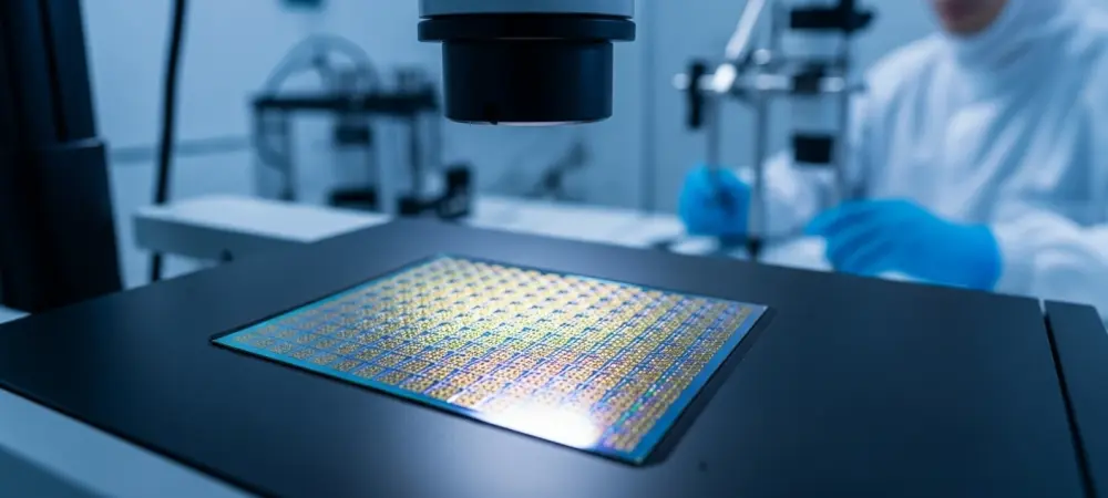
The creation of these high-speed graphene receivers began with the meticulous fabrication of heterostructures involving graphene encapsulated in hexagonal boron nitride (hBN). This encapsulation is a critical step because it protects the graphene from environmental contaminants and minimizes scattering from the substrate, thereby preserving the high carrier mobility necessary for rapid signal detection. The researchers utilized two primary sources for the graphene: high-quality exfoliated flakes for initial proof-of-concept devices and chemical vapor deposition (CVD) grown graphene for evaluating the potential for large-scale manufacturing. These materials were then integrated into a sophisticated architecture designed to maximize light-matter interaction at sub-THz wavelengths.
To solve the problem of graphene’s naturally low absorption in the sub-THz regime, the team integrated resonant on-chip dipole antennas directly onto the graphene channel. These antennas, specifically tuned to a length of approximately 600 micrometers to match the 200–300 GHz carrier frequency, act as concentrators that funnel the electromagnetic energy into a tiny gap where the graphene is located. To further enhance this effect, a silicon-based back mirror was placed beneath the substrate, creating a high-quality optical cavity. This setup allowed the incident radiation to bounce back and forth through the graphene layer, significantly increasing the probability of absorption and the resulting photoresponse.
The detection mechanism itself relies on a split-gate structure that creates a pn-junction within the graphene channel. By applying independent voltages to the left and right gates, a doping asymmetry is established, which facilitates the photothermoelectric (PTE) response. When the sub-THz radiation is absorbed, it heats the electron gas in the graphene, creating a temperature gradient that drives a current across the junction via the Seebeck effect. This process occurs at zero-bias, meaning the device generates its own signal without needing an external power source. The experimental validation of this setup involved a sophisticated dual-laser beating tone system to generate the sub-THz carrier, combined with non-return-to-zero on-off keying (NRZ OOK) modulation to test real-time data transmission and sampling.
Findings
The experimental results provided a robust demonstration of the graphene receiver’s capabilities, most notably the successful transmission of multigigabit-per-second data rates over wireless distances of up to 2.5 meters. This achievement is particularly significant because it was reached without the use of bulky amplifiers or active cooling, relying instead on the intrinsic efficiency of the graphene PTE mechanism. The researchers observed that the eye diagrams—a standard visual tool used to evaluate the quality of a digital signal—remained open and clear at speeds up to 2 gigabits per second, indicating a high signal-to-noise ratio and low bit error rates. In fact, the bit error rate was measured as low as 2.5 × 10⁻⁶, which is well within the thresholds required for reliable digital communication.
One of the most important findings involved the characterization of the trade-off between responsivity and bandwidth. The devices demonstrated a maximum responsivity of 0.16 amperes per watt, which is quite high for a passive 2D material detector. However, the researchers noted that the highest responsivity was typically found in devices with lower bandwidths, around 2 GHz, while other devices achieved setup-limited bandwidths as high as 40 GHz but with lower overall signal strength. This relationship is largely governed by the quality factor of the antenna-cavity system; a stronger resonance traps more energy and increases the signal but also limits the range of frequencies over which the device can respond quickly.
The efficacy of the back-mirror cavity was also quantified, revealing a six-fold increase in field intensity at the graphene junction compared to devices without a mirror. This enhancement was crucial for overcoming the large mismatch between the millimeter-scale wavelength of the sub-THz radiation and the micrometer-scale active area of the graphene sensor. Furthermore, the team validated that the impedance of the graphene channel could be tuned to closely match the standard 50-ohm impedance used in modern microwave and digital electronics. This matching is a vital technical detail because it prevents signal reflections that would otherwise degrade the data rate and increase the complexity of the readout circuitry.
Implications
The implications of this research for the future of mobile technology are profound, particularly concerning power efficiency and device design. Because the graphene receiver operates at zero-bias, it consumes virtually no power during the detection phase, which is a massive advantage for mobile devices where battery life is a primary concern. Most current high-speed detectors require a constant supply of current to operate, which not only drains the battery but also generates heat that must be managed. By eliminating this requirement, graphene enables a much simpler and more compact circuit design, potentially allowing 6G receivers to be integrated into everything from smartphones to wearable health monitors without adding significant bulk.
From a manufacturing perspective, the CMOS compatibility of these graphene devices is a major milestone. Most traditional high-speed semiconductor materials used for THz applications, such as indium phosphide or gallium arsenide, are difficult and expensive to integrate with the silicon wafers that form the backbone of the global electronics industry. Graphene, by contrast, can be grown at a large scale and transferred onto silicon using processes that are increasingly being standardized. This compatibility means that 6G hardware could eventually be produced in the same high-volume factories that make modern computer processors, drastically lowering the cost of the infrastructure needed to support next-generation networks.
Finally, the elimination of complex external matching networks is a subtle but critical benefit. In high-frequency electronics, the connection between different components is often the site of significant signal loss due to impedance mismatches. The ability to design a graphene receiver that naturally matches the 50-ohm standard means that engineers can connect these sensors directly to standard amplifiers and processors with minimal loss. This “plug-and-play” capability simplifies the overall system architecture, making it easier for network equipment manufacturers to adopt graphene technology and integrate it into the next generation of base stations and routers.
Reflection and Future Directions: Analyzing the Next Steps
Reflection
Reflecting on the progress made so far, it is clear that while the results are highly encouraging, several technical constraints remain that must be addressed before wide-scale deployment. One of the primary limitations identified is the role of the antenna-cavity quality factor (Q-factor) in determining the device’s optical bandwidth. While a high Q-factor is excellent for boosting the signal strength through resonance, it also creates a narrow frequency response that can limit the maximum data rate. This creates a challenging engineering dilemma where one must choose between a sensitive receiver with a slower data rate or a faster receiver that requires a much stronger input signal to function correctly.
Another significant challenge encountered during long-distance testing was the issue of signal divergence and free-space losses. Sub-terahertz waves naturally spread out as they travel, and at distances of several meters, the amount of energy actually reaching the tiny graphene sensor can be incredibly small. This was evidenced by the decrease in signal quality and the increase in bit error rates as the distance between the transmitter and receiver was increased to 2.5 meters. Overcoming these losses in a real-world environment, where obstacles and atmospheric changes can further degrade the signal, will require even more sensitive detectors or the implementation of sophisticated beam-forming technologies to keep the radiation focused on the target.
Finally, the performance gap between exfoliated graphene and CVD-grown graphene remains a topic of intense interest. The exfoliated samples used in this study typically showed higher carrier mobility and better overall responsivity because they have fewer defects and grain boundaries. While CVD graphene is much more scalable and suitable for industrial use, its current mobility levels are often lower, which translates to a weaker photoresponse. Closing this performance gap is essential for ensuring that mass-produced 6G chips can match the high standards set by laboratory prototypes. The transition from “hero” devices made in a lab to reliable, high-yield industrial components is always a difficult phase in the development of any new technology.
Future Directions
Looking ahead, the development of broadband antenna designs offers a promising path for increasing data rates beyond current limits. Instead of using a simple dipole antenna with a narrow resonance, future devices could utilize bow-tie or log-periodic structures that are capable of capturing a much wider range of frequencies. This would effectively lower the Q-factor of the system, allowing for much faster response times and higher gigabit-per-second speeds, albeit at the cost of some peak responsivity. Finding the right balance between these factors will be a major focus for engineering teams as they work to optimize these receivers for different types of network environments.
Another exciting direction involves the implementation of Multiple-Input-Multiple-Output (MIMO) arrays. By placing dozens or even hundreds of small graphene receivers on a single chip, it would be possible to significantly improve the overall sensitivity and spatial multiplexing capabilities of the system. This approach, which is already used in 5G and modern Wi-Fi routers, would allow the receiver to capture signals from multiple directions and combine them to create a much more robust and high-speed link. The small footprint and low power consumption of graphene sensors make them ideal for these high-density arrays, which would be difficult to implement with bulkier traditional components.
Finally, continued research into high-mobility scalable graphene growth techniques is vital for the commercial success of this technology. New methods for synthesizing graphene directly on insulating substrates or improving the transfer process from copper foils could help maintain the material’s extraordinary properties even at the wafer scale. If the mobility of industrial-grade CVD graphene can be pushed closer to the levels seen in exfoliated flakes, the responsivity of these receivers will naturally increase, making them even more effective at long-range communication. These advancements, combined with improved encapsulation techniques using materials like transition metal dichalcogenides, will ensure that 2D material-based electronics are ready to meet the rigorous demands of the 6G era.
Advancing 6G Infrastructure Through Graphene Innovation
The successful demonstration of high-speed graphene receivers marks a significant turning point in the quest to overcome the physical limitations that have long hindered the development of sub-terahertz wireless communication. By unifying high-speed detection with a compact, low-power footprint, these devices proved that it is possible to achieve the multigigabit data rates required for 6G without sacrificing portability or energy efficiency. The researchers showed that the strategic integration of resonant antennas and optical cavities could amplify the natural properties of graphene, turning a simple atomic layer into a powerhouse of digital signal processing. This work bridged the gap between fundamental materials science and practical telecommunications engineering, providing a clear roadmap for the next generation of wireless hardware.
The pivotal role of the photothermoelectric effect cannot be overstated, as it enabled a passive, zero-dark-current operation mode that is essentially impossible for traditional semiconductors to replicate at these frequencies. This mechanism allowed for the direct conversion of sub-THz waves into readable electrical signals, simplifying the entire receiver chain and removing the need for power-hungry active components. The result was a system that not only performed at a high level but did so with a degree of simplicity that makes it highly attractive for mass production. As the industry looked for ways to reduce the “Size, Weight, and Power” (SWaP) constraints of 6G infrastructure, graphene-based solutions offered a path forward that met all these criteria simultaneously.
Ultimately, the impact of this innovation extended far beyond the laboratory, offering a final perspective on the indispensable role of 2D materials in the future of semiconductor technology. As traditional silicon-based electronics approached their fundamental physical limits, the introduction of graphene provided a way to bypass these bottlenecks and continue the historical trend of increasing performance. The integration of such novel materials into existing CMOS workflows represented a broader shift in how electronics were designed and manufactured, favoring a hybrid approach that combined the best of established silicon processes with the extreme properties of new atomic-scale layers. This marriage of old and new was the catalyst needed to transition the global communication network into the terabit era, ensuring that the wireless links of the future were as fast, reliable, and efficient as the modern world demanded.
The successful validation of these receivers through bit error rate testing and real-time data streaming provided the final proof needed to move the technology out of the realm of theory and into the world of practical application. By achieving reliable communication over several meters, the research showed that graphene was not just a promising material for the distant future, but a viable solution for the infrastructure challenges being faced today. The development of evaluation kits and integrated printed circuit boards further demonstrated that these sensors could be packaged and deployed in formats that were familiar to industry engineers, lowering the barrier to adoption. As 6G continues to move from a conceptual framework to a physical reality, the innovations described in this research will undoubtedly serve as the foundation for the high-speed, low-latency world that is currently being built.
In conclusion, the journey toward terabit-per-second wireless speeds was a complex endeavor that required a complete rethinking of how we detect and process high-frequency radiation. Through the use of hBN-encapsulated graphene, resonant antennas, and carefully tuned optical cavities, researchers were able to create a new class of receivers that solved the most pressing issues of the 6G era. These devices were low-power, high-speed, and easy to manufacture, making them the ideal choice for the vast networks of sensors and mobile devices that would define the coming decade. The work performed during this investigation set the stage for a new wave of innovation in the field of two-dimensional materials, ensuring that graphene would remain at the forefront of the technological revolution for years to come. The era of sub-terahertz communication was no longer a distant dream but a tangible reality, powered by the unique and extraordinary capabilities of a single layer of carbon atoms.