

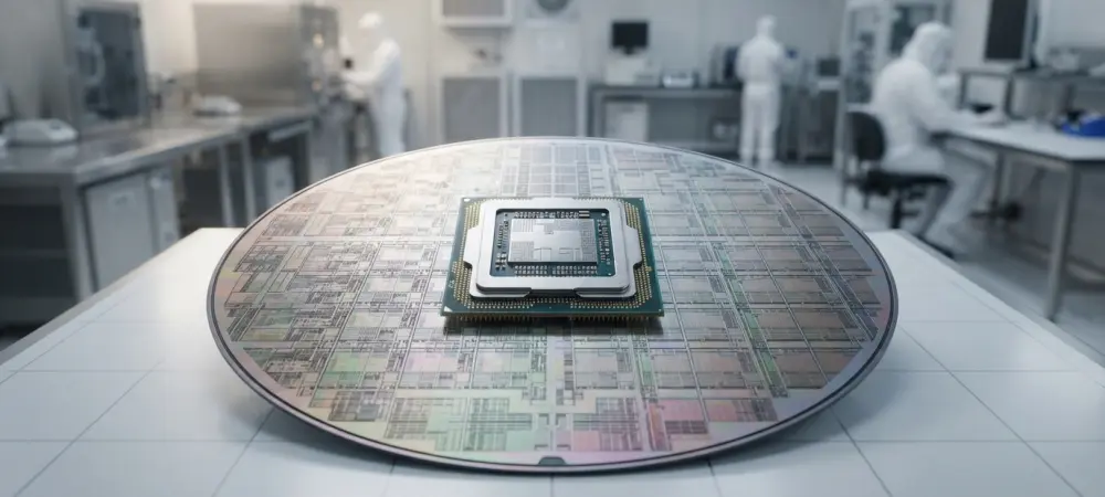
The microscopic architecture defining modern computation has reached a threshold where silicon efficiency is no longer measured merely by raw clock speed but by the sophisticated orchestration of specialized logic units within a single substrate. As the foundational engine of the digital world, the Central Processing Unit (CPU) has undergone a radical metamorphosis, moving away from the monolithic slabs of the past toward heterogeneous, multi-layered systems. This evolution reflects a broader shift in technological priorities, where the ability to process diverse data types—from simple arithmetic to complex neural networks—determines the hierarchy of modern computing performance. The current landscape of 2026 reveals a sector that has successfully navigated the physical limits of silicon by embracing architectural ingenuity, ensuring that the relentless demand for processing power continues to be met through specialization and modularity.
The Fundamental Principles of Modern Processor Design and the Strategic Industry Shift Toward Heterogeneous Computing Architectures
The contemporary processor functions as a highly integrated ecosystem, often referred to as a system-on-a-chip (SoC) rather than a solitary unit of logic. In the current environment, the definition of a CPU has expanded to encompass not just general-purpose cores, but also a suite of specialized accelerators that manage specific workloads with far greater efficiency than a standard arithmetic logic unit (ALU) could ever achieve. This architectural transition was born out of necessity as the industry approached the limits of “Dennard scaling,” the principle suggesting that power density would remain constant as transistors shrank. When this principle began to fail, engineers had to rethink the computer’s “brain,” moving from a jack-of-all-trades approach to a design that prioritizes the right tool for the task.
This fundamental shift is most evident in the way data moves through the internal circuitry of a modern chip, and while the primary objective remains the execution of software instructions, the path those instructions take is now more variable and intelligent than ever before. Modern designs utilize high-speed internal fabrics to connect general-purpose cores with integrated graphics engines, security processors, and memory controllers. This level of integration reduces the latency that previously plagued discrete components, allowing for a seamless flow of information that is essential for real-time responsiveness in everything from mobile user interfaces to industrial automation systems. The modularity of these systems ensures that the processor remains the central nervous system of the device, coordinating a complex symphony of hardware that operates in concert to provide a fluid user experience.
Instruction Set Architecture: The Silent Language of Silicon
The Instruction Set Architecture (ISA) serves as the indispensable bridge between abstract software commands and the physical gates of the processor hardware. It is the definitive contract that dictates how a programmer’s code is interpreted by the silicon, defining the vocabulary of operations available to the machine. Currently, the market is characterized by a fascinating divergence between the legacy-heavy x86 architecture and the power-efficient Arm ecosystem, alongside the disruptive rise of the open-source RISC-V. Each ISA represents a different philosophy of computing, with x86 favoring a Complex Instruction Set (CISC) that prioritizes code density and legacy compatibility, while Arm utilizes a Reduced Instruction Set (RISC) that emphasizes simplicity and lower power consumption per operation.
Despite their differences, the lines between these architectures have blurred significantly in 2026, as high-performance Arm processors now incorporate complex out-of-order execution engines that rival the sophistication of traditional desktop chips. Meanwhile, x86 designs have adopted micro-op translation layers that essentially turn complex instructions into simpler, RISC-like internal operations. This convergence highlights a critical reality in CPU design: the underlying hardware is often far more similar than marketing might suggest. The choice of ISA remains as much a strategic business decision as a technical one, influencing software ecosystems and the long-term viability of hardware platforms. Furthermore, the expansion of RISC-V into the high-performance sector has introduced a new layer of competition, allowing companies to design custom instruction extensions tailored for specific tasks without the licensing burdens of established proprietary architectures.
The Instruction Cycle: Decoding the Path to Execution
The instruction cycle is the fundamental process by which a computer retrieves a program instruction from its memory, determines the required actions, and executes those commands accordingly. This continuous loop is performed by the central processing unit starting from the moment the system boots up until it is eventually powered down.
Fetch Stage
During the fetch stage, the CPU retrieves the next instruction from the system memory. The program counter keeps track of the memory address of the instruction to be processed next, ensuring the sequence remains orderly and efficient.
Decode Stage
Once the instruction is fetched, the control unit interprets the binary code to determine which operation to perform. This stage identifies the necessary operands and the specific internal pathways required to complete the task.
Execute Stage
In the final stage, the CPU carries out the instruction by performing calculations in the arithmetic logic unit or moving data between registers. After execution, the results are stored in memory or registers, and the cycle begins again for the subsequent instruction. The fundamental lifecycle of a processor instruction—Fetch, Decode, and Execute—remains the heartbeat of every computing device, yet the mechanics of this cycle have reached unprecedented levels of complexity. The Fetch unit in a modern CPU is no longer a simple retriever of data; it is an intelligent scout that uses advanced branch prediction algorithms to anticipate the future path of a program. By guessing the outcome of “if-then” logic before it is even calculated, the processor can preload instructions into the pipeline, ensuring that the execution units are never left idle. This speculative behavior is a primary driver of modern performance, effectively hiding the massive latency of system memory by staying several steps ahead of the current task.
Once fetched, the transition to the Decode stage involves a sophisticated translation process; in x86 architectures, this is particularly intensive, as the hardware must identify the boundaries of variable-length instructions before breaking them down into micro-operations. These micro-ops are then fed into a massive reorder buffer, which allows the CPU to execute instructions out of their original sequence if the necessary data is available. This Out-of-Order (OoO) execution is the crowning achievement of modern microarchitecture, enabling the chip to find useful work to do even when a specific thread is stalled. The final Execute stage relies on a vast array of specialized units, including floating-point units for complex math and vector engines for processing large arrays of data simultaneously. This multi-staged pipeline architecture ensures that even though a single instruction might take dozens of clock cycles to complete, the processor can finish several instructions during every single tick of its clock.
Memory Hierarchy and the Quest for Zero Latency
One of the most persistent bottlenecks in CPU architecture is the “memory wall,” which refers to the staggering speed discrepancy between fast processor cores and relatively slow system RAM. To mitigate this, engineers have refined a tiered memory hierarchy that functions like a series of increasingly large and slightly slower staging areas. The Level 1 (L1) cache is the most integrated, located directly within the core to provide nearly instantaneous access to the most vital data. Moving outward, the L2 and L3 caches provide larger pools of storage shared across cores, acting as a buffer that prevents the CPU from having to access the main memory, which is often hundreds of times slower in terms of clock cycles. Innovation in this space has taken a literal turn toward the vertical with the widespread adoption of 3D-stacked memory. By placing additional layers of cache directly on top of the processor logic, manufacturers have been able to expand on-chip storage capacity without increasing the footprint of the silicon die. This “3D V-Cache” technology has proven to be a game-changer for data-intensive applications such as high-fidelity gaming and scientific simulations, where the ability to keep massive datasets close to the execution units results in a dramatic boost in frame rates and computation times. In 2026, the management of this hierarchy is no longer just about size but about intelligent data placement. Modern cache controllers use machine learning-inspired heuristics to predict which pieces of data will be needed next, proactively moving them up the hierarchy to ensure that the execution engines are constantly fed with the information they require.
Innovation Trends: The Dominance of Chiplets and Hybrid Cores
The era of the monolithic chip—where every component is carved from a single, continuous piece of silicon—is rapidly fading into the past, replaced by the modular efficiency of chiplet-based designs. This approach allows manufacturers to mix and match various components manufactured on different process nodes, optimizing for both performance and cost. For example, high-performance cores can be built on the most advanced and expensive 2nm or 3nm nodes, while I/O controllers and memory interfaces, which do not benefit as much from shrinking, can be manufactured on more mature and affordable processes. These individual “tiles” are then joined using advanced packaging technologies, creating a single processor package that is more flexible and yield-efficient than any monolithic predecessor. Complementing this physical modularity is the widespread adoption of hybrid core architectures; by combining large, high-performance “P-cores” with smaller, energy-efficient “E-cores,” modern CPUs can manage their power budget with surgical precision. The P-cores handle demanding foreground tasks like video editing or gaming, while the E-cores quietly manage background processes such as system updates, browser tabs, and network telemetry. This division of labor is managed by a sophisticated hardware-level “thread director” that communicates with the operating system to ensure that every task is assigned to the most appropriate resource. This strategy has not only extended the battery life of mobile devices but has also allowed desktop processors to achieve higher peak performance without overwhelming their thermal solutions, representing a fundamental rethink of how a processor interacts with the software it runs.
Real-World Applications: High-Performance Computing and Data Centers
In the massive server farms that power the global digital infrastructure, CPU architecture is defined by the twin demands of throughput and parallelism. Unlike consumer chips, which focus on low latency for single-threaded responsiveness, server-grade processors are designed to handle thousands of concurrent tasks. This is achieved through massive core counts, sometimes exceeding 128 cores per socket, and a heavy emphasis on memory bandwidth. These chips serve as the backbone for cloud computing, financial modeling, and the vast databases that underpin modern commerce. The primary architectural advantage here is the ability to maintain consistent performance under sustained, heavy loads, a feat that requires immense attention to detail in power delivery and heat dissipation.
Furthermore, the integration of specialized vector and matrix extensions has transformed the server CPU into a powerful tool for data science. While GPUs traditionally handled the heaviest mathematical lifting, modern enterprise CPUs have narrowed the gap by incorporating hardware that can process large batches of data in a single cycle. This makes them ideal for the inference phase of artificial intelligence, where a pretrained model is used to make predictions based on new data. By handling these tasks directly on the CPU, data centers can reduce the complexity of their hardware stacks and improve the overall efficiency of their operations. The ability of the modern CPU to act as both a general-purpose controller and a high-throughput math engine maintains its status as the primary investment for high-performance computing environments.
Artificial Intelligence and the Rise of Local Processing
The most significant architectural shift in recent memory is the deep integration of Neural Processing Units (NPUs) directly into the CPU die. This inclusion marks the transition from cloud-based AI to “Edge AI,” where complex machine learning tasks are performed locally on the user’s device. This is not merely an incremental improvement; it is a fundamental change in the privacy and performance profile of modern computing. By having dedicated silicon for AI workloads, tasks such as real-time language translation, advanced image manipulation, and generative text assistance can occur without sending data to a remote server. This reduces latency, saves bandwidth, and ensures that sensitive user information remains on the device.
The NPU is uniquely designed to handle the repetitive, low-precision math that characterizes neural networks, allowing it to perform these tasks using a fraction of the power required by a traditional CPU core or GPU. This efficiency is critical for the next generation of mobile and “always-on” devices, where the processor must constantly interpret visual or auditory data to provide proactive assistance. In the 2026 landscape, the NPU is no longer an optional luxury but a core component of the architectural blueprint, influencing everything from the way the operating system schedules tasks to the way memory is shared across the chip. This shift represents the industry’s acknowledgment that the future of computing is not just about executing instructions, but about understanding and predicting human intent.
Technical Challenges: Navigating the Physical Limits of Silicon
Despite the rapid pace of innovation, the industry faces daunting physical and economic hurdles that threaten the historical trajectory of performance gains. As transistor features shrink toward the atomic scale, the phenomenon of “quantum tunneling”—where electrons spontaneously jump across insulating barriers—becomes a significant source of power leakage and data corruption. Controlling these errant electrons requires increasingly complex gate geometries, such as Gate-All-Around (GAA) nanosheets, which are both difficult and extremely expensive to manufacture. This has led to a dramatic increase in the cost of developing new process nodes, concentrating the world’s manufacturing capability in the hands of only a few elite foundries.
Beyond the challenges of miniaturization, thermal density has become a primary constraint on architectural design. Modern chips are capable of generating an immense amount of heat in a very small area, creating “hotspots” that can degrade the silicon over time if not managed properly. This has forced a pivot away from simply increasing clock speeds toward improving the “work per watt” of the processor. Furthermore, security has emerged as a critical architectural concern. Vulnerabilities like speculative execution side-channels proved that the very features designed to make CPUs fast could also be used to leak sensitive information. Addressing these flaws requires a fundamental rethink of how the processor handles data privacy at the hardware level, often involving trade-offs that can impact raw performance in exchange for a more secure computing environment.
Market Dynamics: The Competitive Landscape of 2026
The current state of the CPU market is defined by a fierce three-way battle for dominance between established giants and ambitious newcomers. Intel and AMD continue their long-standing rivalry in the x86 space, with each company leveraging different strategies—Intel focusing on its RibbonFET transistor technology and AMD doubling down on its Zen chiplet architecture. However, the true disruptor in recent years has been the expansion of custom silicon by major tech firms. Companies that once purchased off-the-shelf processors now design their own chips based on Arm or RISC-V architectures, tailoring the hardware to their specific software needs. This trend toward vertical integration has shifted the balance of power, as it allows for a level of optimization that was previously impossible.
This competitive pressure has been a boon for innovation, forcing every player in the market to accelerate their development cycles. It has also led to a significant diversification of the hardware ecosystem. We now see specialized processors for every conceivable niche, from ultra-low-power chips for wearable devices to massive, liquid-cooled processors for the most demanding workstations. This fragmentation means that the “best” CPU is now entirely dependent on the specific use case, a reality that has empowered consumers and enterprise buyers alike. The market is no longer a monopoly on a single architecture but a vibrant, albeit complex, landscape where the ability to innovate at the intersection of hardware and software is the ultimate predictor of success.
Future Outlook: Beyond Traditional Silicon and Logic
Looking toward the next horizon, the trajectory of CPU architecture points toward the integration of entirely new materials and computing paradigms. Research into gallium nitride (GaN) and carbon nanotubes suggests that we may soon move beyond the thermal and speed limitations of traditional silicon, allowing for processors that are both faster and more power-efficient. These materials offer superior electron mobility and thermal conductivity, potentially enabling a new era of “cold” computing where high performance does not require massive cooling systems. Additionally, the industry is beginning to explore the integration of optical interconnects, using light instead of electricity to move data between chiplets. This would virtually eliminate the latency and heat generated by copper wiring, allowing for a massive increase in internal bandwidth.
In the long term, the boundaries between the CPU and other forms of computing may continue to dissolve, as we are already seeing the early stages of neuromorphic computing, where hardware is designed to mimic the structure of the human brain’s neural pathways. This could lead to a new class of processors that excel at pattern recognition and sensory processing with almost zero power consumption. Furthermore, while still in its infancy, the potential for coprocessors that leverage quantum mechanical effects to solve specific, highly complex problems remains a tantalizing possibility. The architecture of the future will likely be a “grand unified system,” where classical logic, artificial intelligence, and perhaps even quantum processing exist in a single, cohesive package, ready to tackle the next generation of human challenges.
Summary of the Architectural Landscape
The review of current Central Processing Unit architecture demonstrated that the industry successfully navigated the physical constraints of traditional silicon through the implementation of modularity and specialized logic. The transition from monolithic designs to chiplet-based systems allowed for a more efficient manufacturing process and the flexible integration of heterogeneous components. By prioritizing the development of Neural Processing Units and hybrid core configurations, manufacturers ensured that modern processors could handle the diverse demands of 2026, from local artificial intelligence tasks to high-throughput server workloads. The strategic emphasis shifted from raw gigahertz to intelligent throughput, a change that was necessitated by the cooling and power limitations of densely packed transistors.
Technical hurdles, such as quantum tunneling and thermal hotspots, were mitigated through the adoption of new gate architectures and 3D-stacked memory hierarchies. These innovations provided a necessary bridge as the industry moved toward the end of traditional scaling. The review also highlighted the critical role of Instruction Set Architectures, noting that the competition between x86, Arm, and RISC-V fostered a resilient and varied ecosystem. Ultimately, the architecture of the CPU proved to be a dynamic and evolving field, where the successful integration of hardware and software optimization became the primary driver of performance. The focus now shifted toward exploring exotic materials and optical interconnects to sustain the next phase of global computing growth.