
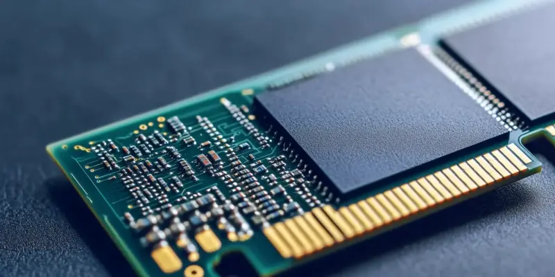
The recently published breakthrough in Magnetoresistive Random-Access Memory (MRAM) by scientists at Osaka University represents a significant leap forward in computer memory technology. This innovation leverages the principles of magnetism rather than electrical currents for data storage, offering potential improvements in both energy efficiency and performance. These advancements could reshape various digital devices, from consumer electronics like smartphones to large-scale data centers. The study, detailed in the journal Advanced Science, highlights the promise of MRAM in addressing longstanding issues in conventional memory systems.
The Basics of MRAM Technology
At the heart of this development is MRAM, distinct from traditional memory technologies which rely on constant power to retain data. Unlike Dynamic Random-Access Memory (DRAM), which requires a continuous electric charge to maintain information, MRAM employs magnetic states, making it non-volatile. This non-volatile nature allows MRAM to sustain stored data even when the power supply is interrupted, similar to how a refrigerator magnet retains its magnetic properties without an external power source. This fundamental attribute of MRAM indicates a drastic reduction in power consumption, particularly during standby modes, effectively resolving one of the major drawbacks of conventional memory systems.
The significant reduction in power consumption means that devices incorporating MRAM can maintain data without continuous energy input. This feature is especially advantageous for battery-operated devices, leading to extended battery life and greater energy efficiency. The non-volatile nature of MRAM also means that data can be instantly available upon powering up the device, eliminating the need for lengthy boot processes. These attributes collectively suggest that MRAM could offer major benefits for a wide array of applications, from personal electronics to critical data infrastructure.
Overcoming Data Writing Challenges
One of the most exciting aspects of this MRAM research is a novel technique to tackle the challenges of data writing. Current MRAM designs still use electric currents for writing data, leading to inefficiencies, particularly as devices miniaturize. These inefficiencies manifest as increased power requirements and heat generation through Joule heating, complicating temperature management as device sizes decrease. Addressing these issues is crucial for the future scalability of MRAM technology in increasingly smaller and more powerful devices.
To circumvent these issues, the Osaka University research team developed an innovative layered structure involving a magnetic material, Co2FeSi, paired with a piezoelectric crystal, PMN-PT. When an electric field is applied to this composite structure, it induces mechanical strain that alters the magnetization direction of the Co2FeSi layer without relying on electric currents. This technique is akin to imprinting patterns with a rubber stamp, where the required force remains consistent regardless of size, allowing data to be written with minimal energy and heat production. This approach significantly reduces the power required for data writing.
The Magnetoelectric Effect and Material Engineering
This new MRAM approach is framed within the context of the magnetoelectric effect – the interaction between magnetic and electric fields within materials. The team demonstrated significant strides in enhancing this effect by precisely engineering the crystal structures of their materials. Through meticulous experimentation, they found that adding an ultra-thin layer of vanadium between the magnetic and piezoelectric layers notably amplified the interaction, improving device stability. This innovative setup allowed them to exhibit a “giant” magnetoelectric effect – a notable achievement in this field.
By refining the thicknesses of the Co2FeSi and vanadium layers to nanometer scales, the researchers achieved exceptionally precise control over magnetic switching behaviors. This control is crucial for the reliable storage and retrieval of data. The research revealed that the MRAM device performed optimally with a 0.3-nanometer-thick vanadium layer and a 30-nanometer-thick Co2FeSi layer, achieving a magnetoelectric coefficient exceeding 10^-5 seconds per meter. These results indicate a leap forward in the practical application of MRAM technology, enhancing its stability and performance under real-world conditions.
Practical Implications and Future Prospects
The creation of this MRAM device employed molecular beam epitaxy, a technique for layer-by-layer material deposition ensuring atomic-scale precision. The resulting layered structures were analyzed using advanced methods such as X-ray diffraction and electron microscopy to confirm their crystalline and magnetic properties. This fundamental approach underscores the importance of material science in pushing the boundaries of memory technology and achieving the high precision needed for practical applications. However, the research also acknowledged that these experiments were conducted on relatively large crystal substrates.
To transition this MRAM technology from the lab to a commercial application, significant advancements in miniaturization and integration will be necessary. The study primarily emphasized fundamental physical properties over immediate practical implementation, suggesting that while the foundational principles are sound, further engineering and development are required to create commercially viable products. This refinement process will involve addressing challenges related to scaling and compatibility with existing manufacturing technologies.
The Future of Non-Volatile Memory Technologies
The overarching trends in this line of research highlight a growing consensus that non-volatile memory technologies like MRAM will be central to future computing innovations. This breakthrough underscores the potential for magnetic materials to transform data storage paradigms, aligning with broader technological goals of sustainability and efficiency in digital devices. As the demands on digital storage continue to grow with the expansion of data-intensive applications, technologies like MRAM offer promising solutions to current limitations.
This innovation could lead to mobile devices with longer battery lives, servers in data centers that consume less power, and generally more energy-efficient computing environments. The ongoing push towards greener technology infrastructures makes the energy-saving potential of MRAM particularly relevant. The researchers involved have made significant strides in reducing the energy costs of memory retention while maintaining high performance, contributing to the development of more sustainable technology solutions.
Support and Recognition
The groundbreaking research on Magnetoresistive Random-Access Memory (MRAM) conducted by scientists at Osaka University marks a significant advancement in computer memory technology. This cutting-edge innovation utilizes the principles of magnetism instead of conventional electrical currents for data storage, which may lead to substantial enhancements in both energy efficiency and performance of digital devices. The potential impact of these improvements spans across a wide range of digital devices, from everyday consumer electronics like smartphones and laptops to massive data centers that drive cloud computing and internet services. The research, published in the journal Advanced Science, emphasizes the promise of MRAM in solving enduring challenges faced by traditional memory systems, including speed, durability, and energy consumption. If widely adopted, MRAM could revolutionize the way data is stored and accessed, paving the way for more powerful and efficient electronic devices. This could be a game-changer for the tech industry, with far-reaching implications for the future of computing and data management.