
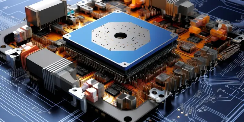
In the fast-paced world of semiconductor technology, the drive to enhance computing power and efficiency has led industry leaders to seek innovative solutions. One such leader, TSMC, has recently unveiled its System-on-Wafer (SoW-X) packaging technology, poised for mass production within two years. This development promises to redefine semiconductor packaging, offering a 40-fold increase in computing power compared to current Chip on Wafer on Substrate (CoWoS) solutions. The journey from CoWoS to SoW represents a leap forward in overcoming the limitations imposed by Moore’s Law, which historically governed the pace of advancements in microchip technology. Moore’s Law, suggesting that the number of transistors on a microchip doubles approximately every two years, is being challenged by the complexities of each successive node, prompting the need for new approaches like the SoW-X packaging.
Transition from CoWoS to SoW-X Technology
CoWoS technology has been instrumental in enhancing computation by integrating multiple chips, or dies, onto a single wafer. This integration allows for more efficient data processing and increased chip capabilities, making CoWoS a pivotal solution for high-performance computing environments. However, TSMC’s transition to the System-on-Wafer technology marks a significant evolution. With the upcoming reticle size expansion reaching up to 9.5x, the CoWoS variant is set to support as many as 12 High Bandwidth Memory (HBM) stacks by 2027, a considerable advancement from the existing 5.5x reticle. This escalation in reticle size facilitates greater data throughput and better overall performance, paving the way for more complex and intensive computing tasks. The progression from CoWoS to SoW-X technology is geared toward larger-scale applications, including artificial intelligence, where massive computational power demands are ever-present.
Advancements and Market Implications
TSMC’s SoW-X technology is notable for its expanded reticle limit, forecasted to boost computational efficiency. It supports up to sixty HBM stacks, catering to high-demand applications like large-scale AI clusters. The capacity to integrate numerous stacks significantly enhances memory capacity and data processing speed, making SoW-X ideal for AI and machine learning challenges. This advancement fortifies TSMC’s market position, setting a new standard in semiconductor packaging innovation. As TSMC pioneers with innovative strategies, the industry may experience widespread adoption and drive further technological progress. The company’s commitment to surpassing traditional barriers charts a dynamic course for future semiconductor innovations, affecting AI-driven technologies and beyond. Overall, the evolution led by SoW-X marks transformative steps in maintaining TSMC’s leadership in this competitive field. With global reliance on advanced computing solutions growing, TSMC’s approach could set a precedent in addressing evolving technological demands, emphasizing efficient and powerful systems while considering environmental and scalability factors pivotal to continuous innovation.