
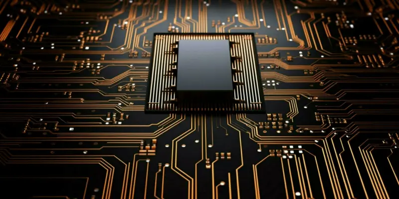
The world of semiconductors is witnessing a groundbreaking transformation with Taiwan Semiconductor Manufacturing Company’s (TSMC) announcement of its 1.4nm-class chips. Scheduled for production in three years, these chips mark a pivotal moment in technological advancement, echoing the immense leap observed with the previous 2nm technology. TSMC’s ambition to transcend traditional barriers in semiconductor design aligns with the shifting priorities from smartphone-centric applications to AI-driven innovations. Their relentless pursuit of perfection promises enhancements in performance and efficiency, largely characterized by improvements in NanoFlex Pro architecture. This evolution reflects the industry’s growing need for more powerful, efficient chips that cater to demanding applications such as data centers, AI accelerators, and client processors. TSMC’s forward-thinking approach is driving an era where semiconductors will redefine computational capabilities on an unprecedented scale.
The Role of Innovative Process Nodes
By embracing advanced process nodes, TSMC is setting a new standard for semiconductor technology. Current ambitions, including the introduction of the A16 node in 2026, establish a roadmap for continuous innovation between existing and future technologies. These interim nodes serve as a bridge to the anticipated A14, embodying incremental but significant strides in performance metrics. At the core of this strategy is the NanoFlex Pro architecture, which allows for enhanced transistor-level optimization. This advancement holds the potential to build upon and possibly surpass the capabilities of the existing FinFlex framework. Such architectural innovations facilitate greater flexibility in power and performance tailoring, essential for meeting the unique demands of different applications. As TSMC integrates these developments into its manufacturing processes, it underscores its role as a pivotal player in the global semiconductor landscape, continuously pushing the boundaries of what’s possible.
Strategic Diversification and Industry Impact
TSMC’s strategic diversification is evident through its comprehensive array of 3nm-class chips, including the N3P and N3X models. Mass production began last year, with the N3P catering to high-performance needs in sectors like data centers. The N3X, on the other hand, aims to provide superior frequency performance and voltage support for applications like client CPUs and AI accelerators. The move from smartphone-centric applications to those focused on AI signals a broader industry shift towards advanced computational demands. Reflecting this change, TSMC’s $40 billion investment by next year demonstrates its commitment to leading semiconductor innovations. By enhancing nodes, TSMC ensures both the continued relevance of cutting-edge fabs and the competitiveness of customer Intellectual Property (IP). This strategy underscores TSMC’s dedication to reshaping the semiconductor industry, profoundly affecting technology’s future. The quest for 1.4nm-class chips promises impactful advancements, setting the stage for progress in efficiency and capabilities.