
The relentless pursuit of mobile processing power often presents a double-edged sword, where groundbreaking advancements in speed and capability can inadvertently introduce unforeseen compromises in other critical areas of performance. As the industry anticipates the arrival of the Samsung Galaxy S26 series, a complex picture is emerging around its heart: the next-generation Exynos 2600 chipset. While this System-on-a-Chip (SoC) is poised to break new ground as the first announced 2nm processor, bringing with it the promise of unparalleled efficiency and performance, whispers from deep within firmware source code suggest an architectural decision that could undermine these very gains. The central concern revolves around a seemingly backward step in chip design, one that could directly impact the one feature every user values above all else: battery life. This potential flaw has cast a shadow over the otherwise bright future of Samsung’s next flagship, creating a narrative of innovation at odds with practicality.
The Architectural Conundrum
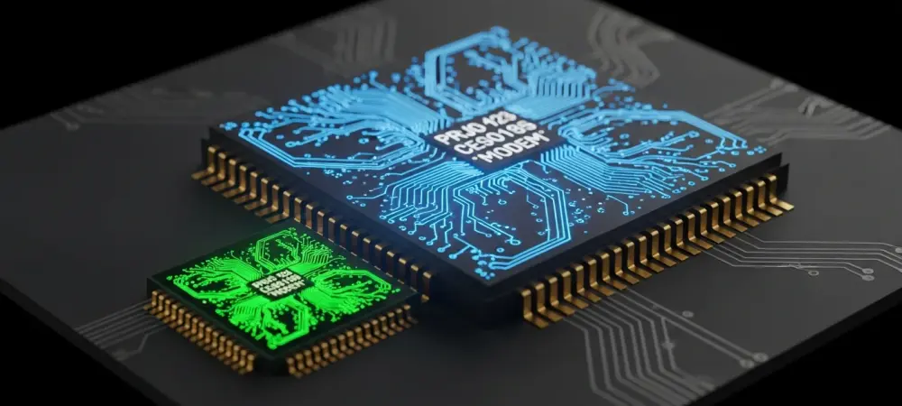
A Step Back in Integration
The announcement of the Exynos 2600 heralded a significant milestone in semiconductor technology, positioning it as the world’s first mobile processor to be built on a 2-nanometer manufacturing process. This leap forward, utilizing advanced Gate-All-Around (GAA) transistor architecture, is designed to deliver a substantial boost in performance while simultaneously reducing power consumption compared to previous generations. In theory, a smaller process node allows for a denser arrangement of transistors, leading to faster signal transmission and less energy leakage—the twin pillars of an efficient and powerful chip. For consumers, this should translate directly into a snappier user experience, enhanced AI capabilities, and, most importantly, longer intervals between charges. The industry has been marching steadily toward this future, where each generational improvement in chip fabrication brings a tangible benefit to the end-user. However, the latest revelations suggest that the Exynos 2600’s design may contain a fundamental compromise that challenges this linear progression toward greater efficiency. Contrary to the long-standing industry trend of integrating as many core components as possible onto a single piece of silicon, evidence suggests the Exynos 2600 will feature a separated, external modem. This insight comes from a detailed analysis of firmware source code, which revealed that the new Shannon 5410 modem component lacks the “AP” (Application Processor) designation typically associated with integrated modems in its predecessors, the Exynos 2500 and 2400. For years, the gold standard in SoC design has been integration, as placing the modem directly alongside the CPU and GPU on the same die minimizes the physical distance data must travel. This proximity reduces latency and, crucially, lowers power consumption. The decision to decouple the modem from the main application processor is therefore a notable and perplexing deviation. It suggests a design constraint, likely related to the overall size and complexity of the 2nm chip, forced engineers to make a concession that could have a direct and negative impact on the device’s power budget.
The Physics of Power Loss
According to semiconductor industry experts, the physical separation of the application processor and the modem is almost guaranteed to result in a less power-efficient system. The core issue lies in the increased distance between their respective interfaces. When these components are on separate chips, electrical signals must travel a longer path, requiring more energy to be transmitted reliably and without degradation. This is not a trivial concern; every data request, from loading a webpage to streaming a video or making a call, involves constant communication between the processor and the modem. Over the course of a day, the cumulative effect of this increased energy expenditure can lead to a noticeable reduction in battery life. This principle holds true regardless of the advanced nature of the processor itself. While the 2nm architecture of the Exynos 2600 will undoubtedly bring its own efficiency benefits, they may be partially or even fully offset by the constant power drain imposed by the external modem design.
This architectural choice was likely not made to enhance performance but was instead a necessary compromise driven by engineering realities. Fabricating a complex, large-scale 2nm SoC with an integrated 5G modem presents immense challenges related to die size, heat dissipation, and manufacturing yield rates. It is plausible that the combined footprint of the advanced CPU/GPU cores and a next-generation modem was simply too large to be produced economically or reliably on a single die. By moving the modem to a separate chip, designers could manage the size and complexity of the main processor more effectively. However, this solution to a manufacturing problem introduces a new problem for the user. It represents a trade-off where the pursuit of cutting-edge processing power came at the expense of holistic system efficiency, creating a potential bottleneck that could define the battery experience for millions of Galaxy S26 owners.
Mitigating the Fallout
A Battery-Sized Solution
In an apparent effort to counteract the potential efficiency losses from its chip architecture, Samsung is reportedly planning a tangible upgrade to the power source of its entry-level flagship. Leaks indicate that the standard Galaxy S26 model is slated to receive a battery capacity increase, moving from the 4,000mAh cell in its predecessor to a more substantial 4,300mAh battery. This represents a 7.5% boost in raw capacity, a figure that appears carefully calculated to offset the anticipated increase in power consumption. This move can be interpreted as a direct acknowledgment of the external modem’s impact. Rather than relying solely on software optimizations or the inherent efficiency of the 2nm process, the company seems to be opting for a brute-force solution: adding more fuel to the tank. For prospective buyers of the base S26, this could be welcome news, as it may neutralize the modem’s negative effects and result in a battery life that is on par with, or perhaps slightly better than, the previous generation.
This strategy, however, is not without its own set of trade-offs. A larger battery physically occupies more internal space, potentially leading to a thicker or heavier device, and adds to the bill of materials, which can affect the final retail price. It signifies a hardware-based compensation for what is fundamentally an architectural challenge. While effective, it suggests that the power drain from the separated modem is significant enough to warrant a physical redesign of the phone’s internal layout. This preemptive measure indicates that Samsung’s engineers are fully aware of the potential for a negative user experience and are taking concrete steps to mitigate it before the device even reaches production. The larger battery in the Galaxy S26 is therefore not just a routine yearly upgrade but a crucial component in a delicate balancing act between next-generation performance and real-world usability.
A Tale of Two Tiers
While the base model may be receiving a hardware solution to its potential battery woes, the situation appears markedly different for the premium tiers of the lineup. Current information suggests that the Galaxy S26+ and S26 Ultra will not benefit from a similar battery capacity increase, retaining the same 4,900mAh and 5,000mAh batteries as their S25 counterparts. This creates a deeply concerning scenario for customers considering these more expensive models. These devices are expected to leverage the full power of the Exynos 2600 for more demanding tasks, from advanced camera processing to high-performance gaming, all of which place a greater strain on the battery. If the external modem’s power consumption negates the efficiency gains of the 2nm process, these flagship phones could experience a net decrease in battery life compared to the models they are replacing. This would be a significant regression, particularly in a premium market where longevity and reliability are paramount expectations.
This discrepancy in strategy could create a perplexing value proposition for consumers. Those who pay the most for the top-tier Ultra and Plus models might paradoxically receive a device with a compromised battery experience relative to the previous year’s flagships. Such an outcome could prove to be a significant challenge from a marketing perspective, as it would be difficult to champion the performance of a new chip if it comes at the cost of daily endurance. For Samsung, it sets up a potential imbalance within its own product line, where the most advanced and feature-rich phones are also the most vulnerable to a core architectural flaw. The decision to forgo a battery upgrade in the premium models suggests a confidence that software optimization and the 2nm process will be sufficient, a gamble that may or may not pay off when the devices are subjected to real-world use.
An Anxious Wait for Real-World Performance
The engineering decisions surrounding the Exynos 2600 ultimately created a complex narrative of both innovation and compromise. The choice to separate the modem from the main processor, while likely a necessary trade-off to manage the complexities of 2nm manufacturing, introduced a significant variable into the critical battery life equation. The proposed countermeasure—a larger battery for the base model—highlighted the company’s awareness of the potential efficiency shortfall but simultaneously raised pointed questions about the user experience for the premium-tier devices. As the details emerged, the industry and consumers were left to anticipate whether the theoretical performance gains of a groundbreaking new process node would be enough to overcome the tangible efficiency costs of a fragmented chip architecture.