
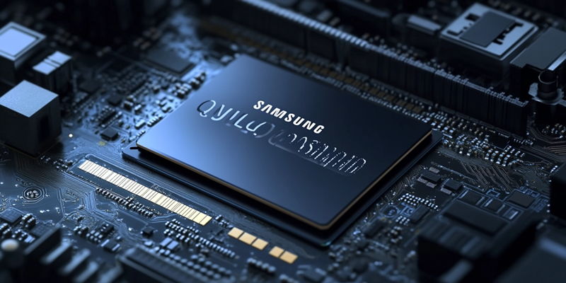
Samsung has introduced its 9th generation quad-level cell (QLC) V-NAND flash storage, pushing the envelope in solid-state storage technology. The primary focus of this innovation is on capacity enhancement rather than performance. This new generation of QLC NAND, designed to meet the high-capacity demands of artificial intelligence (AI) applications, features the highest number of layers in QLC flash history. Though Samsung did not specify the exact number of layers, it is speculated to be between 280 and 290 layers, a significant increase from the 236 layers of the 8th generation V-NAND.
Technological Breakthroughs
Surpassing the 1-Terabit Threshold
A notable breakthrough is Samsung surpassing the 1-terabit (Tb) threshold for QLC flash, paving the way for more affordable high-capacity SSDs, potentially up to 8 terabytes (TB). The development involves Samsung’s advanced techniques, such as channel hole etching and a double-stack structure, facilitating the stacking of two high-layer dies using string stacking technology. This technological advancement has not only boosted storage density by 86% but also considerably enhanced write performance through predictive technology for cell state changes. These improvements ensure that the 9th generation QLC V-NAND is not only larger but more reliable and faster than previous iterations.
The implications of surpassing the 1-Tb threshold extend beyond mere capacity. By dramatically increasing the amount of data a single chip can store, Samsung is opening doors for mass storage solutions that are not only viable for consumer electronics but also for enterprise-level applications. High-density, efficient storage solutions are crucial for the burgeoning fields of big data, machine learning, and other data-intensive applications. With the enhanced write performance, even massive datasets can be managed efficiently, reducing latency and improving overall system productivity.
Enhancing Power Efficiency
Moreover, the new QLC V-NAND demonstrates a significant reduction in power consumption, with a 30% decrease in read operations and a 50% reduction in write operations compared to the 8th generation. This results in better efficiency, making it an attractive option for data centers and AI-driven applications requiring large data repositories. Lower power consumption translates to lower operational costs and a smaller carbon footprint, aligning with the broader industry trend towards greener, more sustainable technology solutions. This is particularly significant as data centers, often dubbed the “backbone of the internet,” increasingly strain global energy resources.
The increased power efficiency also means that devices utilizing these NAND chips will have longer battery life, a crucial factor for mobile and portable devices. In environments where power availability can be limited or inconsistent, such as remote data acquisition stations or mobile data centers, the reduction in power consumption can be a game-changer. By addressing one of the major pain points in data storage—energy efficiency—Samsung not only offers a high-performing product but also a cost-saving and environmentally friendly solution.
Industry Impact
Commitment to Innovation
Samsung’s continuous innovation in NAND technology reflects a broader trend towards increasing storage capacities and improving power efficiency. The company’s advancements underscore a commitment to addressing the growing data storage needs driven by AI and other advanced technological applications. Through these innovations, Samsung solidifies its leadership in the flash memory market, setting new benchmarks for storage capacity, efficiency, and performance. By pushing the envelope in NAND technology, Samsung is not just responding to current market demands but also anticipating future needs, thereby maintaining its competitive edge.
This commitment to innovation is also seen in Samsung’s ongoing investment in research and development. The leap from 236 layers in the 8th generation to potentially 290 layers in the 9th generation is a testament to the company’s dedication to pushing technological boundaries. Such advancements do not occur overnight but are the result of sustained effort, significant financial investment, and a forward-thinking approach. Samsung’s relentless pursuit of excellence ensures that it remains at the forefront of technological advancements, influencing industry standards and driving the market forward.
Future Prospects
Samsung has unveiled its 9th generation quad-level cell (QLC) V-NAND flash storage, setting new standards in solid-state storage technology. This latest development prioritizes increasing storage capacity over optimizing performance. It aims to meet the substantial demands for higher capacity storage driven by artificial intelligence (AI) applications. One of the standout features of this new QLC NAND is its unprecedented number of layers, which is the highest ever in QLC flash history. While Samsung has not disclosed the precise number of layers, it is estimated to range between 280 and 290, marking a significant leap from the 236 layers found in the 8th generation V-NAND. Moreover, this enhancement not only signifies a monumental increase in data storage capabilities but also highlights Samsung’s commitment to advancing technology to address the evolving needs of AI and other data-intensive applications. This breakthrough is expected to have a considerable impact on various industries that rely heavily on massive data processing and storage solutions.