
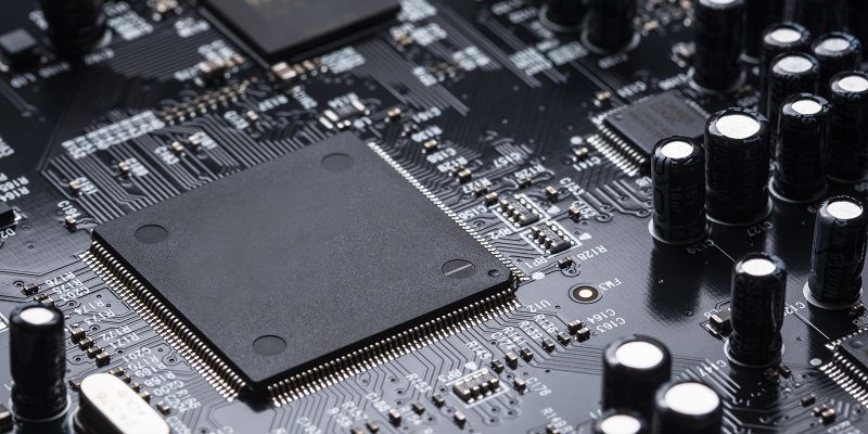
In a groundbreaking announcement at the VLSI Symposium held in Japan, Samsung Electronics unveiled its latest innovation in power delivery technology. The new method, known as Backside Power Delivery Network (BSPDN), promises to revolutionize chip design by improving area utilization and power delivery efficiency. Samsung’s disclosure marks a significant milestone in the industry, as they become the first company to reveal the metrics and results of this pioneering technique.
Samsung’s Disclosure at the VLSI Symposium
At the highly regarded VLSI Symposium, Samsung Electronics took the opportunity to illustrate the benefits of the BSPDN method. By presenting detailed metrics and data, the company showcased the remarkable achievements made in both area reduction and power delivery enhancement.
Area reduction achieved
One of the key highlights of Samsung’s BSPDN innovation is the impressive area reduction it offers. By implementing this method, the company was able to reduce the required chip area by a staggering 14.8% compared to the traditional approach. This reduction provides Samsung with the opportunity to utilize the freed-up space to incorporate additional components, such as transistors, driving overall performance gains.
Performance benefits of area reduction
The area reduction achieved through BSPDN has far-reaching implications for chip performance. With more space available on the die, chip designers can integrate additional components, improving functionality and delivering faster processing speeds. This enhancement opens up new possibilities for innovation in a wide range of applications, from mobile devices to high-performance computing.
Wire length reduction and improved power delivery
In addition to area reduction, Samsung’s BSPDN method also yields significant benefits through wire length reduction. By optimizing the power delivery network on the backside of the chip, the company achieved a commendable wire length reduction of 9.2%. This reduction translates into decreased resistance and improved power delivery efficiency, ensuring stable and reliable operation of the semiconductor device.
Samsung leads the way in disclosure
Samsung’s disclosure of the BSPDN method at the VLSI Symposium demonstrates its leadership in pushing the boundaries of chip design and manufacturing. By sharing its findings, the company contributes to the collective knowledge of the industry and fosters further innovation in power delivery techniques.
Intel’s Similar PowerVia Method and Integration Plans
Not long after Samsung’s revelation, Intel also disclosed its own power delivery innovation called “PowerVia.” Intel intends to incorporate this method into its Intel 20A nodes, achieving an impressive 90% chip utilization rate. The company has already announced plans to utilize PowerVia in their upcoming Arrow Lake CPUs, slated for release in 2024. Intel’s utilization of this methodology emphasizes its significance and potential for industry-wide adoption.
Samsung’s Future Plans for BSPDN Integration
While Samsung’s disclosure of the BSPDN method showcases its remarkable capabilities, the company has not yet revealed its concrete plans for integrating this technology into its future processes. However, based on the information available, it is expected that next-generation processes will gradually incorporate BSPDN after Intel’s initial implementation.
Samsung’s unveiling of the BSPDN method at the VLSI Symposium has ushered in a new era of power delivery innovation in chip design. The remarkable achievements in area reduction and power delivery enhancement present numerous benefits, including increased performance, improved power efficiency, and the potential for incorporating more features into semiconductor devices — all contributing to a faster and more advanced technological landscape. As the industry eagerly awaits the adoption of BSPDN and similar advancements, it is clear that Samsung and Intel’s breakthroughs lay the foundation for a promising future in microelectronics.