
Nvidia, a leading technology company specializing in graphics processing units (GPUs) and artificial intelligence (AI), has made a significant move by placing an order with Taiwan Semiconductor Manufacturing Company (TSMC) for 3nm wafers. This order serves as the foundation for Nvidia’s highly anticipated Blackwell architecture, signaling a new era in chip design. In this article, we will delve into the details of this order and explore the implications of Nvidia’s groundbreaking decision.
Nvidia’s flagship design: GB100
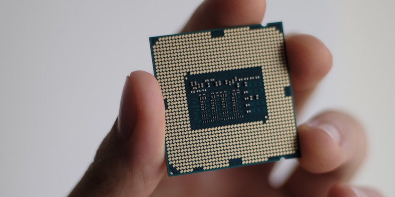
At the forefront of Nvidia’s Blackwell architecture lies the GB100, the company’s flagship chip for high-performance computing (HPC) and AI. The GB100 represents Nvidia’s dedication to pushing the boundaries of innovation and delivering exceptional computational power. As Nvidia continues to dominate the AI market, the GB100 is poised to become a game-changer in advancing technologies such as machine learning and data analytics.
Timeline for release
According to reports, Nvidia plans to release its compute offerings, including GB100, in the last quarter of 2024. This ambitious timeline reflects Nvidia’s commitment to staying ahead in the competitive semiconductor industry. However, it also poses challenges and expectations in terms of meeting customer demand and delivering state-of-the-art products within the designated timeframe.
Changes expected with Blackwell architecture
It is widely anticipated that almost every facet of Nvidia’s design will undergo transformation with the introduction of the Blackwell architecture. This extends beyond performance improvements to encompass fundamental alterations in architecture, power consumption, and scalability. While specific details remain under wraps, industry experts are eagerly awaiting Nvidia’s unveiling of Blackwell to witness the revolutionary changes it will bring.
The need for chiplet design
With the AI market expanding rapidly, Nvidia is reaching the limits of modern fabrication capabilities, encountering challenges with its massive monolithic designs. To overcome these limitations, the company has opted for a chiplet design for GB100. This approach involves dividing the chip into smaller modular components, allowing for improved flexibility, performance, and efficient use of resources. However, it remains unclear if this approach will extend to Nvidia’s GeForce dies, which cater to the gaming market.
Selection of 3nm Process
While Nvidia has placed an order for 3nm wafers with TSMC, it is yet to be disclosed which specific process Nvidia will select. TSMC offers a menu of different 3nm designs to its customers, presenting Nvidia with multiple options that must be carefully evaluated. The final decision will have a significant impact on the overall performance and efficiency of Nvidia’s future chips, signaling an exciting technological crossroad for the company.
Competition and Collaboration
Nvidia’s move towards the Blackwell architecture and its order for 3nm wafers align with industry trends. Intel, one of Nvidia’s key competitors, is expected to join in soon with its upcoming integrated GPU (iGPU) tiles. Additionally, AMD, another major player in the semiconductor market, is rumored to collaborate with TSMC for both Zen 5 and RDNA 4 designs. These developments underscore the significance of Nvidia’s order as the race for chip supremacy intensifies.
Prioritization of AI Chips
Given the exponential growth of AI applications, there is speculation that Nvidia may start prioritizing AI chip development over gaming cards in the future. This strategic shift reflects the company’s commitment to meeting the increasing demand for AI-enabled technologies across various industries. While this move holds immense potential, it raises questions about the impact on Nvidia’s gaming-centric customer base and its ability to balance both markets effectively.
Packaging bottleneck challenges
Nvidia’s transition to chiplet designs, coupled with TSMC’s recent challenges with packaging bottlenecks, adds complexity to the current landscape. As more companies adopt chiplet designs, the demand for advanced packaging technologies increases, potentially exacerbating TSMC’s ongoing struggle to meet customer demands. Addressing the packaging bottleneck will be crucial to sustain the industry’s rapid innovation pace and ensure timely product deliveries.
Nvidia’s order for 3nm wafers from TSMC marks a significant milestone in the company’s journey towards the Blackwell architecture. The upcoming release of GB100, Nvidia’s flagship chip for HPC and AI, promises to revolutionize the industry by pushing the boundaries of computational power even further. As Nvidia navigates the evolving landscape of chip design, the choices made in selecting the 3nm process and addressing packaging challenges will shape the company’s competitive position. With rapid advancements in AI and increasing market demand, Nvidia’s strategic decisions hold the potential to reshape the semiconductor industry for years to come.