

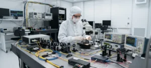
The establishment of the Terahertz and Hybrid Semiconductor Chips Competence Center in Vilnius represents a pivotal moment for European technological leadership and the broader evolution of wireless communication systems. This state-of-the-art facility is not merely a laboratory but a strategic response to the increasing demand for data-intensive applications that current 5G infrastructures struggle to support. By focusing on the intersection of high-frequency electronics and advanced material science, the initiative seeks to define the architecture of the 6G era.
The importance of this development lies in its focus on the “Terahertz Gap,” a segment of the electromagnetic spectrum that holds the key to unprecedented wireless speeds. As global networks face congestion, the move toward higher frequencies becomes a necessity for maintaining the pace of digital transformation. This center serves as the foundational pillar for Lithuania’s contribution to the global telecommunications ecosystem, bridging the gap between theoretical physics and industrial application.
A Quantum Leap Into the Terahertz Era
The race for 6G connectivity is fundamentally a race to master the 100-349 GHz frequency range, a domain where traditional silicon-based components often fail to perform efficiently. Moving beyond the limitations of existing 5G infrastructure requires a specialized understanding of how waves behave at these extreme frequencies, where atmospheric absorption and signal scattering present significant engineering hurdles. The debut of the Terahertz and Hybrid Semiconductor Chips Competence Center in Lithuania provides the specialized environment needed to test these high-frequency boundaries.
Harnessing this frequency range is essential because it offers the massive bandwidth required for real-time holographic communication and ubiquitous artificial intelligence. While lower frequencies are reliable for wide-area coverage, the terahertz frontier provides the “data highways” necessary for short-range, ultra-high-speed bursts of information. This research is pivotal for ensuring that the transition to the next generation of wireless technology is not just an incremental update but a genuine revolution in how devices interact with the physical world.
The Strategic Importance of Semiconductor Autonomy
Developing advanced materials is the primary method for overcoming the physical obstacles inherent in high-frequency transmission. The center prioritizes semiconductor autonomy, ensuring that the critical components for future networks are designed and fabricated within a secure, domestic supply chain. This focus on advanced materials allows for the creation of chips that can handle the thermal and electronic stresses of terahertz waves, effectively bridging the divide between the immense speeds of fiber-optic cables and the mobility of wireless devices. This initiative bolsters the European Union’s pursuit of digital sovereignty by reducing reliance on external technology providers for critical infrastructure. In an era where infrastructure resilience is a matter of national security, having the capability to produce specialized 6G hardware locally is a significant strategic advantage. By controlling the design process from the atomic level up to the integrated circuit, the center ensures that European connectivity remains robust, secure, and technologically independent.
A Multi-Disciplinary Architecture for Next-Gen Connectivity
Engineering integrated detectors and receivers for high-frequency data harvesting requires a sophisticated blend of photonic and electronic techniques. The center utilizes Gallium Nitride (GaN) platforms, which are celebrated for their superior wave modulation capabilities and high-power efficiency compared to traditional semiconductors. These platforms are essential for creating the compact, high-performance transceivers that will eventually be embedded in everything from urban light poles to mobile handsets.
Moreover, the research extends to utilizing structured light to break the 100-meter transmission barrier, a distance that has traditionally limited the utility of terahertz waves. By developing photonic waveguide innovations, the center is creating a seamless interface where light and radio waves can be converted with minimal loss. Scientists are also modeling ultrafast processes within these semiconductor materials to ensure that as data speeds increase, the reliability and scalability of the hardware remain intact for commercial use.
European Leadership and the Human-Centric Tech Vision
The financial backing for this center is part of a broader €630 million Horizon Europe public investment strategy aimed at securing the continent’s technological future. A close collaboration between Vilnius University and the Physical and Technological Sciences Center ensures that academic breakthroughs are rapidly translated into market-ready solutions. This synergy is vital for maintaining a competitive edge in a global market where the speed of innovation is the primary currency.
Expert perspectives at the center emphasize a “privacy-by-design” approach, which integrates security protocols directly into the hardware of 6G systems. This human-centric vision ensures that the next generation of connectivity prioritizes the protection of personal data and the establishment of global security standards. By synthesizing individual scientific achievements into a unified technological framework, the center provides a blueprint for international markets that value both performance and ethical technology standards.
Navigating the Path to 6G Implementation
The transition toward 6G required a fundamental rethinking of how hardware interacted with dense urban environments where physical obstructions often disrupted terahertz signals. Engineers established a roadmap that prioritized the integration of these new chips into existing telecommunications ecosystems to ensure a cost-effective transition between 2026 and 2030. This strategy focused on hybrid systems that utilized existing 5G towers as a backbone while adding high-frequency small cells to handle localized data surges in smart cities.
The center also addressed the practical challenges of commercialization by streamlining the move from laboratory research to industrial production. New insights into energy-efficient modulation helped lower the operational costs of high-frequency networks, making them more attractive to global carriers. Ultimately, the work conducted at this center laid the groundwork for international standards that reconciled the demand for extreme speed with the necessity of sustainable, secure, and accessible data transmission for all citizens.