
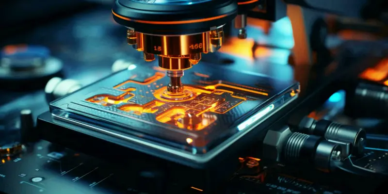
In a world where the demand for computing power continues to surge, Intel’s newest semiconductor process, the 18A, represents a groundbreaking leap in technology. Unveiled at the 2025 VLSI Symposium, this novel process is set to transform the semiconductor landscape with its impressive enhancements over Intel’s previous node, Intel 3. Central to this innovation are the integration of RibbonFET (GAA) transistors and PowerVia technology, which collectively promise substantial performance gains. Notably, Intel’s CEO, Pat Gelsinger, has been explicitly prioritizing the foundry division, signifying a strategic push towards vertical integration of the supply chain and setting high expectations for what Intel could achieve in this arena.
Technological Advancements
Intel’s 18A process boasts more than a 30% increase in density scaling, alongside a 25% boost in operational speed and a remarkable 36% reduction in power consumption when running at 1.1 volts on a standard Arm core sub-block. These figures highlight the significant efficiency and performance improvements enabled by the 18A process. Notably, the RibbonFET technology, a gate-all-around (GAA) approach, enhances the control over transistor channels, leading to better performance metrics. On the other hand, PowerVia technology addresses power delivery issues, ensuring more stable power under high-performance conditions by shortening paths between transistors and power sources.
The underlying advancements are also supported by Intel’s collaboration with IMEC, particularly in the domain of hybrid bonding and through-dielectric vias. These innovations contribute to the higher density and better power characteristics, making hybrid bonding essential for vertical stacking in advanced semiconductor designs. This combination of techniques underscores the critical role of partnerships in pushing semiconductor technology forward and maintaining a competitive edge.
Competitive Landscape
As Intel continues to spearhead these technological innovations, the competitive dynamics within the semiconductor industry become increasingly intriguing. The 18A process aligns closely with TSMC’s N2 process in terms of SRAM density, which signifies Intel’s ability to match, if not surpass, its primary industry competitor. This competitive parity is a significant achievement for Intel, considering the intense race to achieve smaller, more efficient nodes among leading semiconductor companies. One of the major points of Intel’s 18A process is its implementation in upcoming products. Intel’s new processors, including the Panther Lake SoCs and the Xeon “Clearwater Forest” CPUs, are slated to be the first to utilize this advanced node. These processors will likely appear in commercial and consumer markets by 2026, assuming Intel maintains their yield rates and ramps up to mass production targets. This timeline is critical, as it not only showcases Intel’s engineering capabilities but also affects the broader market dynamics, influencing the rollout of next-generation computing devices and services.
Strategic Implications
Intel’s advancements with the 18A process underscore the company’s strategic maneuver to regain leadership in the semiconductor sector. The potential for vertical integration of the supply chain, highlighted by CEO Pat Gelsinger, could enable Intel to streamline production, reduce dependency on external suppliers, and potentially lower costs. This strategic approach might also enhance responsiveness to market changes, fostering more dynamic and agile product development cycles. Moreover, the 18A process symbolizes Intel’s commitment to pushing the envelope in semiconductor innovation. It offers a glimpse into the future of computing, where enhanced performance, power efficiency, and scalability are not just corporate goals but industry-wide expectations. This forward-thinking mindset is essential for maintaining relevance in a rapidly evolving technological landscape, where the bar for innovation continues to rise.
Conclusion and Future Outlook
In a world where the demand for computing power is constantly increasing, Intel’s latest semiconductor process, the 18A, signifies a monumental advancement in technology. Introduced at the 2025 VLSI Symposium, this new process is poised to revolutionize the semiconductor industry with significant improvements over its predecessor, Intel 3. Key to this innovation are the adoption of RibbonFET (GAA) transistors and PowerVia technology, which together promise notable performance enhancements. Importantly, Pat Gelsinger, Intel’s CEO, has been explicitly emphasizing the importance of the foundry division. This focus highlights Intel’s strategic move towards vertical integration within its supply chain, setting ambitious goals for the company’s potential achievements in this domain. By prioritizing vertical integration, Intel aims to streamline its operations, reduce reliance on external suppliers, and improve overall efficiency, positioning itself as a leader in semiconductor manufacturing and pushing the boundaries of what is possible in the industry.