
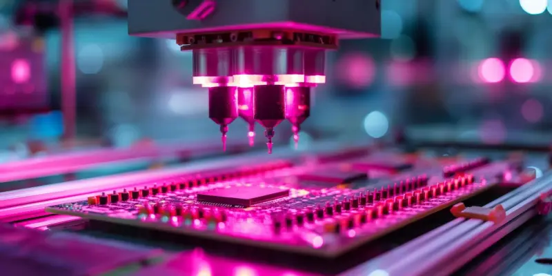
Semiconductor technology has always been at the forefront of innovation, pushing the boundaries of what’s possible in electronics. As demands for more powerful and compact devices grow, the industry is shifting from traditional 2D semiconductor chips to more advanced 3D designs. This transition poses significant challenges, particularly in the precise alignment of multiple stacked layers. Researchers at the University of Massachusetts Amherst have developed a groundbreaking laser-based method to address these alignment issues, promising to revolutionize 3D chip manufacturing.
Challenges in 3D Chip Manufacturing
The Shift to 3D Designs
Historically, semiconductor chips were manufactured in two dimensions, with components laid out on a flat surface. However, as devices become more sophisticated, the limitations of 2D designs are becoming increasingly apparent. The industry is moving towards 3D chip designs, which involve stacking multiple 2D layers to create compact and powerful processors. This new approach allows for improved performance, reduced power consumption, and smaller form factors but introduces the critical need for precise alignment of each layer. Misalignments in 3D chip manufacturing can have severe consequences. Even minimal misalignments can lead to significant performance degradation or complete failure of the chip. Traditional alignment methods involve manually aligning marks on the chip layers using a microscope. This method is time-consuming and prone to errors due to the physical gap between the layers and the need to refocus repeatedly.
Traditional Alignment Methods
Traditional methods for aligning chip layers involve using a microscope to manually align specific marks such as corners or crosshairs on the layers. This approach has several inherent limitations. The physical gap between layers requires constant refocusing, which can introduce further misalignments. Additionally, manual alignment is labor-intensive and can lead to operator fatigue, increasing the risk of errors. Attempts to automate this process have had limited success, often resulting in compromised accuracy or increased complexity and cost. These challenges have created a bottleneck in the production and scaling of 3D chips, limiting their widespread adoption despite their advantages. The need for a more precise, efficient, and cost-effective alignment method has become increasingly urgent.
Laser-Based Alignment Method
The Role of Concentric Metalenses
The new technique developed at UMass Amherst leverages the power of lasers and advanced optics to achieve unprecedented precision in aligning 3D chip layers. Central to this method are concentric metalenses, specially designed optical elements that manipulate light at a microscopic scale. Each chip layer is embedded with alignment marks made of these metalenses.
When a laser is projected through these metalenses, it creates holograms corresponding to the exact position of the marks. The holograms from different layers interfere with each other, producing an interference pattern. This pattern provides clear visual feedback on the alignment status, indicating both the direction and magnitude of any misalignment with remarkable precision.
Achieving Unprecedented Precision
The laser-based method’s precision has exceeded expectations, allowing for the detection of misalignments as small as 0.017 nanometers horizontally and 0.134 nanometers vertically. This level of accuracy is orders of magnitude better than traditional methods. The technique not only improves alignment precision but also reduces the time and effort required for the process. This breakthrough has significant implications for the semiconductor industry. Improved alignment precision can enhance chip performance, increase yield rates, and reduce wastage, leading to lower production costs. Furthermore, the method’s simplicity and efficiency make it accessible to a broader range of manufacturers, including smaller companies and startups, potentially democratizing advanced chip manufacturing.
Implications and Future Applications
Impact on the Semiconductor Industry
The implications of this laser-based alignment technique extend beyond improving alignment precision. By addressing one of the most persistent and costly challenges in 3D chip manufacturing, this innovation can significantly impact the industry’s landscape. Manufacturers can produce more reliable and performant chips, accelerating the adoption of 3D designs in various applications, from consumer electronics to high-performance computing. Lowering the technical and financial barriers associated with ultra-precise chip alignment opens new opportunities for innovation and competition. Smaller firms and startups can now venture into advanced chip manufacturing without incurring prohibitive costs, fostering a more dynamic and diverse industry ecosystem.
Potential for Broader Applications
Beyond chip manufacturing, the researchers at UMass Amherst suggest that their laser-based alignment technique could be adapted for various other applications. Compact, low-cost sensors are one such potential area. The precision of the alignment method could be utilized to develop advanced sensors for pressure, vibration, and other environmental monitoring purposes. These sensors could find applications in various fields, including medical devices, automotive systems, and industrial monitoring. The ability to produce highly accurate and reliable sensors at a lower cost could drive innovation across multiple industries, leading to new products and technologies that benefit society as a whole.
Towards a Brighter Future in Chip Manufacturing
Semiconductor technology has consistently driven innovation, pushing the limits of what’s achievable in electronics. With the demand for more powerful and compact devices on the rise, the industry is transitioning from conventional 2D semiconductor chips to more sophisticated 3D designs. This shift brings with it considerable challenges, notably in achieving precise alignment of the multiple stacked layers within the 3D structures.
In response to these challenges, a team of researchers at the University of Massachusetts Amherst has pioneered a novel laser-based technique to resolve these alignment issues. Their groundbreaking method promises to significantly enhance the process of manufacturing 3D chips. The precision and efficiency offered by this laser-based solution could revolutionize the way 3D semiconductor chips are produced, offering higher performance and smaller form factors for future electronic devices. This advancement holds the potential to change the landscape of electronics and propel the industry into a new era of innovation.