
In an era where performance and efficiency are paramount, AMD continues to push the boundaries with its latest Zen 5 CPU architecture. The new Ryzen 9000 "Granite Ridge" CPUs mark a significant step forward in computing technology. This article delves into the specific advancements of the Zen 5 CPUs, examining how they promise to revolutionize future computing performance.
The Core of Zen 5: Architectural Advancements
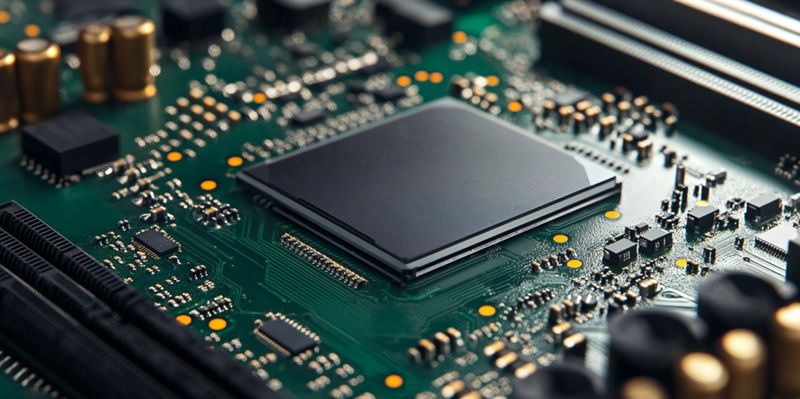
High-Resolution Die Shots: A Closer Look
Fritzchens Fritz’s high-resolution die shots showcase the architecture and intricate design of the Zen 5 CPU. These images reveal the meticulous engineering that defines AMD’s latest processor, offering a visual understanding of its innovations. The Zen 5 CCD, with a die size of 70.6mm² and housing 8.315 billion transistors, represents a notable leap from its predecessors. By utilizing TSMC’s N4P process node, AMD can pack more transistors into a smaller area, enhancing performance and efficiency.
The intricate details captured in these die shots are not just for visual appeal; they provide a comprehensive understanding of the architectural depths of Zen 5. This kind of inspection has historically been pivotal for analysts and enthusiasts who aim to grasp the nuances of CPU design advancements. The sheer density of transistors packed into such a modest die size echoes AMD’s continued emphasis on pushing silicon to its limits. By adopting TSMC’s next-gen fabrication process, AMD underscores its commitment to leveraging cutting-edge technology to push out CPUs that are not just faster but also more power-efficient.
TSV Reduction: Streamlined Design
One of the standout features of the Zen 5 architecture is the reduced number of Through Silicon Vias (TSVs). This reduction signifies a shift towards a more streamlined design, which is pivotal for performance optimization. Fewer TSVs mean less thermal and structural stress on the CCD, translating to better stability and potentially longer lifespan for the CPU. This design choice illustrates AMD’s commitment to refining and improving its core technologies without significantly driving up production costs.
By focusing on reducing the number of TSVs, AMD has likely managed to achieve better thermal management and overall structural integrity of the CPU. TSVs are crucial in connecting various layers of the chip, but they also add complexity and potential points of failure. By minimizing these, AMD can not only improve the robustness of their CPUs but also potentially increase the chips’ lifespan. This streamlined approach ensures that the processors can handle more intensive workloads without overheating or suffering from structural degradation over time.
Innovations in 3D V-Cache Technology
Potential for 2-Hi Stacked 3D V-Cache
Another critical aspect of the Zen 5 architecture is the speculation around the integration of a 2-Hi stacked 3D V-Cache design. This innovation could drastically improve data processing speeds and overall computational efficiency. While 3D V-Cache can considerably boost performance, integrating this technology is not without challenges. The 2-Hi design aims to counterbalance the stress on the CCD, showcasing AMD’s dedication to pushing technological boundaries.
The introduction of a 2-Hi stacked 3D V-Cache could mean significantly lower data latencies and enhanced cache bandwidth, directly translating to superior overall CPU performance. However, stacking layers also introduces challenges like heat dissipation and structural stability. By resolving these issues, AMD demonstrates its engineering prowess and commitment to pushing the boundaries of what’s technically feasible. This ability to maintain technological progression amid challenges showcases AMD’s unswerving focus on innovation, aiming to bring transformative changes in how CPUs handle complex data processing tasks.
Mainstream vs. High-End Models
The possible inclusion of 3D V-Cache in AMD’s product lineup brings up interesting discussions about market positioning. While it may enhance high-end CPU models, mainstream CPUs like the Ryzen 7 series may not feature this advanced cache due to cost constraints. This strategic decision underscores the balance AMD must maintain between cutting-edge technology and market viability. It suggests that while Zen 5 CPUs will deliver groundbreaking performance, the most advanced features might be reserved for premium offerings.
Differentiating the high-end models from the mainstream variants allows AMD to offer products at various price points, ensuring that cutting-edge technology remains accessible yet top-tier performance is preserved for those willing to invest more. By potentially reserving 3D V-Cache for higher-end models, AMD can avoid inflating the production costs of their mainstream offerings, keeping them competitive. This balanced approach enables AMD to cater to a broad spectrum of users, from enthusiasts and professionals to everyday consumers requiring robust computational capabilities without premium costs.
Broader Implications of Zen 5 Advancements
Extending Innovations Across Product Lines
The architectural insights gained from the Zen 5 die shots will extend beyond the Ryzen 9000 series. AMD plans to incorporate these advancements into other product lines, such as Strix, Fire Range, Kraken, and various Turin models. This widespread integration demonstrates AMD’s holistic approach to innovation, ensuring that their latest technologies benefit a broad spectrum of devices and applications.
Extending Zen 5’s architectural advancements across various product lines ensures that AMD’s cutting-edge technology influences a wide array of devices. This approach reflects AMD’s holistic innovation strategy aimed at improving performance uniformly across their entire product portfolio. Such integration of advancements not only solidifies AMD’s position in the high-performance computing space but also extends the benefits of more efficient and powerful CPUs to a diverse range of users. Whether it’s high-performance workstations or consumer-level desktops, these innovations are poised to provide tangible benefits.
Balancing Innovation with Cost
While the architectural advancements in Zen 5 are groundbreaking, AMD faces the inherent challenge of balancing innovation with production costs. The reduced number of TSVs and potential 3D V-Cache integration are excellent for performance but can introduce complexity and fragility in the manufacturing process. This complexity can make high-end models more expensive, necessitating careful consideration of cost versus benefit in AMD’s product strategy. By carefully selecting which innovations to incorporate into each product tier, AMD aims to deliver cutting-edge performance while remaining competitive in the market.
Striking the right balance between incorporating advanced features and maintaining cost-effective production processes is crucial for AMD. It ensures that while the latest technological advancements are integrated, the end products remain viable and accessible across different market segments. By judiciously choosing which innovations to include in each product tier, AMD effectively manages to offer a range of CPUs that cater to different user needs and budgets. This strategic balancing act allows AMD to uphold its reputation for delivering high-performance computing solutions while ensuring sustainability and profitability.
Technical Specifications and Performance Metrics
Transistor Density and Die Size
The technical specifications of the Zen 5 CPUs are impressive. With 8.315 billion transistors packed into a 70.6mm² die, the processor showcases an incredible density, made possible by the advanced TSMC N4P process node. This high transistor density is a key driver of the Zen 5’s enhanced performance capabilities. It allows for more computational power within a compact and efficient design, pushing the limits of what AMD CPUs can achieve.
The transistor density achieved through TSMC’s N4P fabrication process underscores how far AMD has pushed the envelope. This high transistor count not only boosts processing power but also enhances energy efficiency, enabling CPUs to deliver more performance per watt. The compact size of the Zen 5 die facilitates quicker data transfer rates, minimizing latency and maximizing output efficiency. This architectural brilliance underscores AMD’s commitment to delivering powerful, efficient chips capable of handling the most demanding computational tasks with ease.
Computational Efficiency Gains
In an age where high performance and efficiency are essential, AMD relentlessly advances the field with its cutting-edge Zen 5 CPU architecture. The introduction of the Ryzen 9000 "Granite Ridge" CPUs signifies a remarkable leap forward in computing technology. This article explores the groundbreaking innovations of the Zen 5 CPUs, shedding light on how they are set to transform future computing landscapes.
It’s vital to understand the technical refinements that make Zen 5 stand out. The new Ryzen 9000 series doesn’t just offer incremental improvements; it represents significant advancements in processing power, energy efficiency, and overall system performance. By employing a more efficient 5-nanometer process, AMD has managed to pack more transistors into a smaller space, thereby drastically enhancing the computational capabilities of each chip.
Additionally, the revamped architecture includes smarter cache management and improved multi-threading performance, which collectively contribute to faster data processing and more responsive multitasking. These features make the Zen 5 CPUs particularly well-suited for demanding applications, from gaming to professional creative software.
Overall, AMD’s Zen 5 CPUs are poised to revolutionize how we approach computing tasks, making them faster and more efficient than ever before.