
A New Dimension in the Global Chip War
In the high-stakes arena of artificial intelligence, where Nvidia has long been the undisputed champion with its advanced GPUs powering the world’s most sophisticated AI models, a strategic pivot designed to sidestep limitations is being orchestrated by China. Facing escalating US export controls that restrict access to cutting-edge semiconductor technology, Chinese technologists are “building upward” by pioneering a chip stacking strategy that integrates less advanced, domestically producible components into powerful, multi-layered systems. This article explores the technical underpinnings, strategic rationale, and formidable challenges of this approach, analyzing whether this innovative architectural gambit can realistically challenge Nvidia’s entrenched AI leadership and reshape the future of high-performance computing.
Forged in Fire The Geopolitical Roots of a New Strategy
To understand China’s pivot to chip stacking, one must first grasp the geopolitical pressures shaping its semiconductor industry. For years, the global standard for performance was dictated by Moore’s Law—a relentless race to shrink transistors on a single silicon die. This race is won in the world’s most advanced fabrication plants, or “fabs,” using extreme ultraviolet (EUV) lithography machines that China is barred from acquiring due to stringent US-led sanctions. This has created a technological ceiling, effectively locking Chinese firms out of the sub-7nm process nodes where industry leaders like Nvidia, supplied by TSMC, thrive. This reality has forced a strategic reckoning: competing head-on in a race it is prevented from winning is futile. The chip stacking initiative is therefore not just a technical choice but a pragmatic adaptation born of necessity—a strategic shift from a frontal assault on fabrication leadership to an asymmetric campaign focused on architectural design and advanced packaging.
Deconstructing China’s Vertical Ambition
The Technical Blueprint Building Upward with Mature Nodes
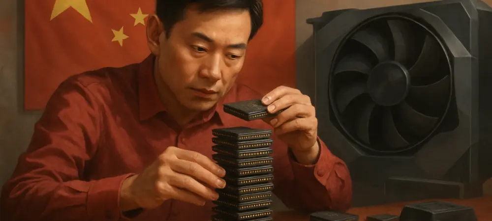
At the heart of China’s strategy lies the concept of 3D integration, a departure from traditional 2D chip design. Championed by industry proponents, the proposed architecture involves vertically stacking multiple dies—such as 14nm logic chips and 18nm DRAM—into a single, cohesive unit. This approach is critically enabled by two core innovations. The first is a “software-defined near-memory computing” paradigm, which physically places processing cores and memory in close proximity to slash the latency and energy costs of data movement—a primary bottleneck in AI workloads. The second is the use of 3D hybrid bonding, an advanced packaging technique that creates direct, ultra-dense copper-to-copper connections between the stacked layers. This method forms a seamless, high-bandwidth interconnect that is far more efficient than conventional packaging, effectively turning a collection of mature chips into a single high-performance system.
A Reality Check on Performance Ambition vs Physics
While the architectural concept is sound, the performance claims have been met with healthy skepticism. Proponents suggest that a stacked 14nm configuration could achieve a performance of 120 TFLOPS (trillion floating-point operations per second), putting it in the same league as Nvidia’s top-tier GPUs. However, a direct comparison reveals a significant gap. Nvidia’s A100 GPU, a workhorse of the AI industry built on a more advanced process node, delivers up to 312 TFLOPS. This 2.5x performance deficit highlights a fundamental truth: architectural ingenuity cannot entirely negate the laws of physics. Advanced nodes like 4nm and 5nm offer superior transistor density, greater power efficiency, and better thermal characteristics. Stacking older, hotter, and less efficient 14nm chips creates immense design challenges and cannot magically replicate the raw computational power derived from smaller, more advanced transistors.
Sidestepping the CUDA Moat and Strategic Sanctions
Perhaps the most brilliant aspect of the chip stacking strategy is how it addresses Nvidia’s most formidable competitive advantage: its CUDA software ecosystem. For over a decade, Nvidia has cultivated a vast and loyal community of developers who build AI applications on its CUDA platform. Any competitor with a traditional GPU architecture faces the monumental task of either replicating CUDA or convincing this community to switch. China’s approach cleverly sidesteps this dilemma. By creating a novel near-memory computing architecture, it necessitates the development of a completely new, bespoke software stack. While a colossal undertaking, this move changes the rules of the game, avoiding a direct and unwinnable comparison with CUDA and instead attempting to build a new ecosystem from the ground up, tailored specifically to its unique hardware. This embodies the philosophy of focusing on “stacking” to achieve system-level performance where direct competition is impossible.
The Road Ahead Hurdles and Future Horizons
The path to realizing this vision is fraught with immense technical challenges that will define its ultimate success. The most critical hurdle is thermal management. Stacking multiple heat-generating 14nm logic dies creates a dense thermal hot spot that is incredibly difficult to cool, risking system instability and performance throttling. Furthermore, manufacturing yields for complex 3D packages are notoriously low; a single defect in any of the stacked layers can render the entire expensive unit useless. Beyond the hardware, the creation of a robust and user-friendly software ecosystem—including compilers, libraries, and developer tools—is a multi-year, resource-intensive endeavor that will ultimately determine whether the hardware’s potential can be unlocked. Despite these obstacles, this strategy could carve out a niche in specific applications like AI inference or data analytics, where memory bandwidth is often a greater bottleneck than raw compute, paving the way for a more diverse hardware landscape.
Strategic Takeaways for a Shifting Industry
The primary insight from China’s chip stacking initiative is that innovation in high-performance computing is no longer solely defined by transistor shrinkage. The industry is entering an era where system-level design, advanced packaging, and hardware-software co-optimization are becoming primary drivers of performance. For businesses and technology leaders, the key takeaway is to look beyond process nodes as the only metric of progress. This development signals that alternative, heterogeneous computing architectures are a viable response to supply chain restrictions and geopolitical pressures. Observers should not dismiss this strategy as a mere stopgap but recognize it as a legitimate, albeit challenging, path toward semiconductor self-sufficiency and a potential source of architectural disruption in specialized markets.
Conclusion Redrawing the Lines of AI Competition
China’s chip stacking strategy was a compelling testament to adaptive innovation in the face of immense pressure. It was not a silver bullet that immediately dethroned Nvidia, as significant performance and ecosystem gaps remained. However, it represented a calculated and intelligent pivot away from a direct confrontation in fabrication technology toward a new competitive front in system architecture. By shifting the battlefield to areas like advanced packaging and software design, China attempted to rewrite the rules of the game. This strategic maneuver ensured that the future of AI hardware would not be a monolithic race to the smallest transistor but a multifaceted competition where architectural diversity and ingenuity played a decisive role in shaping the next generation of computing.