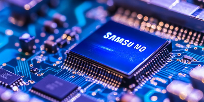
Samsung is gearing up to revolutionize storage technology with its next-generation 400-layer Vertical NAND (V-NAND). The new memory architecture aims to significantly enhance data storage capacity and reliability. This initiative follows Samsung’s recent mass production of its 9th-gen V-NAND, which adopted Quad-Level Cell (QLC) technology to improve performance, capacity, and dependability. The upcoming 10th-gen V-NAND is expected to launch in 2026, boasting a 400-layer configuration—an impressive 43% increase over its predecessor’s 280 layers. To accomplish this feat, Samsung will employ Bonding Vertical (BV) NAND technology, which diverges from the existing Circuit on Periphery (CoP) design. While CoP places peripheral circuits atop the memory stack, the BV method involves initially manufacturing memory and peripheral circuits separately and then vertically bonding them. This approach minimizes circuit damage during stacking and could achieve nearly 60% higher bit density, resulting in substantial capacity increases within the same physical space. Samsung’s method is akin to YMTC’s Xtacking and Kioxia-Western Digital’s CMOS Bonded Array technologies.
Redefining Storage Technology
Samsung’s leap to a 400-layer V-NAND architecture marks a significant milestone in the storage technology landscape. By adopting the BV method, Samsung has the potential to redefine storage capabilities, enabling higher density without increasing the physical footprint of storage devices. This transformation is not just about adding more layers; it introduces a way to produce more memory cells within the same silicon wafer area, thereby making data storage more efficient. Samsung’s new V-NAND technology is expected to improve read and write speeds, which are crucial for applications requiring fast data access, such as high-performance computing and real-time data processing.
Beyond capacity, the new architecture also promises enhanced reliability and durability. The separation of memory and peripheral circuits reduces the likelihood of damage during manufacturing, which in turn could lead to longer-lasting storage solutions. For enterprises relying on vast amounts of data, this reliability translates into lower maintenance costs and reduced downtime. As the digital world continues to produce an exponential amount of data, innovations like Samsung’s 400-layer V-NAND will be pivotal in meeting future storage demands. The challenge will be in seamlessly integrating this advanced technology into existing storage systems and ensuring compatibility with current and future data management frameworks.
Future Innovations
Samsung is set to transform storage technology with its upcoming 400-layer Vertical NAND (V-NAND). This new memory design aims to vastly improve data storage capacity and reliability. This advancement comes after Samsung’s recent release of its 9th-generation V-NAND, which utilized Quad-Level Cell (QLC) technology to boost performance, capacity, and reliability. The forthcoming 10th-generation V-NAND, expected in 2026, will feature a 400-layer structure, a notable 43% increase from its current 280 layers. To achieve this, Samsung will implement Bonding Vertical (BV) NAND technology, which differs from the current Circuit on Periphery (CoP) design. While CoP places peripheral circuits on top of the memory stack, the BV method involves separately manufacturing memory and peripheral circuits, then bonding them vertically. This minimizes circuit damage during stacking and could enhance bit density by nearly 60%, leading to significantly increased capacity in the same physical space. Samsung’s approach is similar to YMTC’s Xtacking and Kioxia-Western Digital’s CMOS Bonded Array technologies.

