
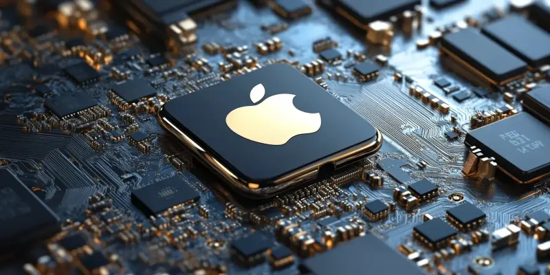
In a bold move toward advancing its chip technology, Apple is poised to make significant changes to its upcoming M5 silicon chips, departing from the previously used unified memory architecture. Noted analyst Ming-Chi Kuo has revealed that all M5 variants, including the base M5, M5 Pro, M5 Max, and M5 Ultra, will be fabricated using TSMC’s cutting-edge 3nm N3P process node. This marks a notable improvement from the existing N3E node utilized in the M4 and A18 Bionic chips. The most noteworthy transformation, however, could be the shift towards a split CPU/GPU memory architecture. Since the M1’s debut, Apple’s silicon has leveraged a unified memory pool shared between CPU and GPU cores. This design has been celebrated for delivering excellent performance-per-watt efficiency, particularly in MacBooks. The move away from this architecture may introduce additional complexity but could also provide significant performance enhancements for specific workloads.
The new memory architecture promises exciting yet demanding changes for both developers and Apple. Unified memory architecture facilitated a streamlined flow of data between CPU and GPU, reducing latency and improving efficiency. Shifting to a split memory configuration may provide dedicated bandwidth to CPU or GPU-specific tasks, possibly leading to improvements in graphics rendering and computational tasks. With the increased complexity of managing separate memory pools, developers might need to adapt their software to harness the full potential of this new architecture.
Advanced Packaging Technology
To accommodate this groundbreaking architectural change, Apple plans to leverage TSMC’s advanced 2.5D packaging technology, SoIC-mH. This technology employs innovative 3D stacking and hybrid wafer bonding techniques to create ultra-dense chip connections. Unlike traditional 3D vertical stacking, SoIC-mH allows for the horizontal attachment of separate dies to the package. This methodology promises not only better yields but also superior thermal performance. Effective heat dissipation has been a paramount concern in chip design, especially as processing power increases. Superior thermal management afforded by advanced packaging could be crucial in realizing the performance potential of the new M5 architecture.
One of the intriguing aspects of this packaging technology is its compatibility with Apple’s ambitious Private Cloud Compute focus, which emphasizes AI processing power. The enhanced performance and adaptability of these new chips could be pivotal in handling the intense computational demands of AI applications. By ensuring that the chips remain cool and functional under heavy workloads, Apple is setting the stage for a new era of performance and reliability that aims to support major advancements in AI and machine learning capabilities.
Projected Timelines and Strategic Shifts
Apple is gearing up for major changes in its chip technology, particularly with its forthcoming M5 silicon chips. According to analyst Ming-Chi Kuo, all M5 variants—including the base M5, M5 Pro, M5 Max, and M5 Ultra—will be crafted using TSMC’s state-of-the-art 3nm N3P process node. This signifies a notable upgrade from the existing N3E node used in M4 and A18 Bionic chips. The most significant change, however, may be the transition to a split CPU/GPU memory architecture.
Since the M1’s release, Apple’s silicon has utilized a unified memory pool shared between CPU and GPU cores, celebrated for its excellent performance-per-watt efficiency, especially in MacBooks. Moving away from this architecture might introduce added complexity but could also result in significant performance enhancements for certain workloads. The new memory design promises exciting yet demanding changes for both developers and Apple. Unified memory architecture streamlined data flow between CPU and GPU, reducing latency and boosting efficiency.
Switching to a split memory setup might offer dedicated bandwidth for CPU or GPU-specific tasks, potentially improving graphics rendering and computational tasks. However, the increased complexity of managing separate memory pools means developers might need to adapt their software to fully harness this new architecture’s potential.