

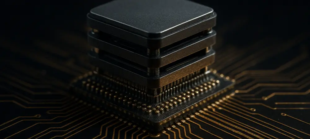
The geographical concentration of advanced logic production is currently undergoing its most radical realignment since the dawn of the digital age as capital flows toward Europe. Advanced Micro Devices (AMD) has initiated a definitive transformation of the semiconductor landscape with a $10 billion investment focused on expanding its presence in Germany. This move represents a fundamental departure from the traditional reliance on concentrated manufacturing hubs in East Asia, aiming instead to build a robust, localized infrastructure capable of sustaining the next decade of computational growth. The primary objective of this massive capital injection is to develop a state-of-the-art manufacturing and research campus that addresses the explosive demand for artificial intelligence and high-performance computing. By establishing this facility, the organization is not merely adding capacity but is actively diversifying its global footprint to ensure supply chain continuity in an increasingly fragmented world.
This market analysis explores how the $10 billion expansion serves as a cornerstone for European technological independence while solidifying a competitive advantage in the race for AI dominance. The relevance of this move cannot be overstated, as it touches upon the critical intersection of industrial policy, advanced engineering, and international trade dynamics. Readers will gain insights into the specific technical innovations being localized in Germany, such as advanced 3D packaging and modular chip designs, which are essential for the next generation of data center hardware. Furthermore, the analysis examines the broader socioeconomic implications, including the creation of a massive high-tech workforce and the strengthening of academic and industrial synergies within the region. This investment marks a turning point where regional resilience becomes as valuable as raw processing power.
As the industry looks from 2026 to 2030, the success of this initiative will likely determine the balance of power in the silicon market. The following sections detail the historical context that necessitated this shift, the localized economic benefits, and the technical hurdles that this new facility is designed to overcome. By prioritizing geographic diversification, the strategy provides a blueprint for risk management that other sectors are already beginning to emulate. This analysis ultimately underscores the necessity of public-private cooperation in securing the hardware foundations of the modern digital economy, providing a comprehensive view of why this $10 billion commitment is the most significant industrial event in the current European landscape.
Historical Realignment: From Fragility to Regional Resilience
The semiconductor industry has historically operated under a model of extreme centralization, where a handful of manufacturing hubs produced the vast majority of the world’s advanced logic. For decades, this efficiency-first approach served the global market well, providing cheap and plentiful silicon for consumer electronics and enterprise hardware. However, the early years of this decade exposed the profound vulnerabilities inherent in such a concentrated system. Logistical failures, regional instabilities, and unexpected surges in demand created a global bottleneck that paralyzed industries ranging from automotive manufacturing to telecommunications. These challenges highlighted the urgent need for a shift toward “geographic resilience,” where production is distributed across multiple stable regions to prevent a single point of failure from derailing the global economy.
Germany, and specifically the region known as Silicon Saxony, has long stood as a bastion of European microelectronics expertise, making it the most logical site for this massive $10 billion pivot. The area already possesses a sophisticated ecosystem of materials suppliers, equipment manufacturers, and specialized researchers, providing a foundation that would take decades to build from scratch elsewhere. Historically, the region has transitioned from a localized manufacturing center to a global player in power electronics and sensor technology. AMD’s decision to plant deeper roots here is an evolution of this history, scaling the existing expertise to meet the more rigorous demands of 5-nanometer and 3-nanometer production. This background is essential for understanding why the current investment is seen as a maturation of the European tech sector rather than a speculative venture.
The lessons learned from previous supply chain disruptions have fundamentally altered how multinational corporations view long-term infrastructure. In the current market, “just-in-time” manufacturing is being replaced by “just-in-case” regionalization. This historical shift matters because it dictates where the most advanced research and development funding will be allocated over the coming years. By moving production closer to the massive European data center and automotive markets, the organization is effectively shielding itself from the volatility of international shipping and trade disputes. This strategic realignment ensures that the foundations of AI and cloud computing remain secure, regardless of the shifting political tides in other parts of the world.
Economic and Structural Transformation: The German Silicon Expansion
Workforce Development: High-Tech Employment and the Multiplier Effect
The immediate economic impact of the $10 billion investment in Germany is expected to ripple through the regional economy, creating a massive wave of high-value employment. Conservative estimates project the creation of approximately 4,000 direct roles within the new facility, focusing on specialized disciplines such as photolithography, chemical engineering, and silicon validation. These are not merely administrative positions; they represent a significant increase in the regional density of doctoral and master’s-level talent. However, the true scale of the impact lies in the “multiplier effect,” which industry analysts suggest will generate roughly five indirect jobs for every direct hire. This includes everyone from the construction teams building the specialized cleanrooms to the logistics providers managing the delicate transport of raw wafers and finished components.
Beyond the raw numbers, the expansion is triggering a modernization of the regional infrastructure to support a facility of this magnitude. German authorities are working in tandem with the private sector to upgrade power substations and high-purity water treatment plants, which are critical for the resource-intensive process of chip fabrication. These upgrades serve the broader community as well, providing a modernized utility grid that can attract further high-tech investment. The project is being treated as a cornerstone of national industrial strategy, with streamlined regulatory pathways that demonstrate a newfound agility in European governance. This collaborative environment is essential for maintaining the aggressive construction schedule required to meet the production goals set for the near future.
The development of this workforce also addresses a critical talent gap that has plagued the technology sector for several years. By offering high-paying, stable careers in a specialized field, the project encourages a new generation of students to pursue advanced degrees in STEM fields. Local vocational schools and universities are already recalibrating their curricula to align with the specific technical needs of the new facility, ensuring a steady pipeline of talent. This structural shift in the labor market not only benefits the semiconductor industry but also elevates the overall technological capability of the region, making it more competitive against other global innovation hubs. The presence of such a large-scale employer provides a level of economic stability that can withstand broader market fluctuations, anchoring the regional economy for decades.
The Frontier of Heterogeneous Integration: Advanced Packaging Initiatives
A central technical objective of the German expansion is the establishment of a world-class center for advanced packaging and heterogeneous integration. As the industry approaches the physical limits of traditional transistor scaling, the focus has shifted from making individual chips smaller to making collections of chips work together more efficiently. This involves “chiplet” architectures, where various specialized components—such as processors, graphics engines, and high-bandwidth memory—are manufactured separately and then integrated into a single high-performance unit. The new facility will be at the forefront of these 3D stacking technologies, which are vital for the Instinct MI series accelerators and other high-end hardware.
By localizing these complex processes in Europe, the organization can more effectively serve the specific needs of the region’s growing AI ecosystem. The ability to integrate different process nodes within a single package allows for unprecedented design flexibility and energy efficiency. This is particularly important for the European market, where energy costs and sustainability regulations are among the most stringent in the world. The German site will serve as a laboratory for these modular manufacturing methods, proving that high-performance silicon can be produced with a lower environmental impact and a more agile delivery cycle. This technical lead is a key differentiator in a market where performance-per-watt has become the most important metric for data center operators.
The shift toward chiplet-based designs also offers significant advantages in terms of manufacturing yield and cost control. In traditional monolithic designs, a single defect can ruin an entire large chip; however, with modular packaging, only the individual faulty chiplet is discarded, significantly improving overall efficiency. The German facility’s expertise in this area will allow for faster iterations of hardware, enabling the company to respond more quickly to the rapidly evolving requirements of AI training and inference models. This focus on the “back-end” of production—once seen as a secondary concern—is now recognized as the primary engine of innovation in the semiconductor industry, making the German site a critical node in the global technology chain.
Knowledge Clusters: Synergizing Industry with Academic Innovation
The $10 billion investment extends far beyond the factory floor, as a significant portion of the capital is dedicated to long-term research and development within a collaborative ecosystem. By consolidating European R&D activities into a single massive campus, the company is bridging the traditional gap between theoretical breakthroughs and industrial-scale application. Strategic partnerships with world-renowned institutions, including the Technical University of Munich and various branches of the Fraunhofer Society, are being established to explore the next frontier of computing. These collaborations are focused on high-priority areas such as energy-efficient edge AI, quantum-resistant security, and photonic interconnects, which could eventually replace traditional electrical wiring on chips.
These knowledge clusters are essential for fostering a culture of continuous innovation that extends beyond the immediate product roadmap. When academic researchers have access to industrial-grade fabrication tools and real-world data, the pace of discovery accelerates significantly. Conversely, the industry benefits from a fresh influx of ideas and a rigorous scientific approach to problem-solving. This synergy is particularly effective in Germany, where the “Mittelstand” tradition of specialized engineering provides a unique backdrop for large-scale corporate research. The goal is to create a self-sustaining cycle of innovation where today’s laboratory experiments become tomorrow’s commercial hardware, ensuring that the region remains at the cutting edge of the global digital economy.
Furthermore, these research initiatives are addressing some of the most misunderstood aspects of modern computing, such as the actual environmental cost of AI. Through joint programs with local environmental scientists, the R&D teams are developing new cooling technologies and power-management algorithms that could drastically reduce the carbon footprint of massive data centers. By positioning itself as a leader in “green silicon” and ethical AI hardware, the organization is aligning its technical trajectory with the values and regulatory expectations of the European market, creating a long-term strategic advantage that is difficult for competitors to replicate.
Silicon Sovereignty: Navigating the Geopolitics of Future Production
The pursuit of silicon sovereignty has become a defining theme of the late 2020s, as nations and regional blocs realize that their economic security is inextricably linked to their ability to produce advanced processors. The $10 billion investment in Germany is perfectly aligned with the broader goals of the EU Chips Act, which seeks to secure the continent’s technological future by doubling its share of global chip production. This policy environment has been instrumental in making the expansion financially and logistically viable, providing a framework for subsidies and infrastructure support that offsets the higher costs of manufacturing in Europe. As we look toward 2030, this trend of regionalization is expected to intensify, with other major economies launching similar initiatives to protect their own digital supply chains.
Environmental sustainability is also becoming a key battleground in the race for technological leadership. Future manufacturing facilities will no longer be judged solely by their nanometer process or clock speeds, but by their water usage, energy efficiency, and carbon neutrality. The German project is setting a high bar in this regard, utilizing the country’s robust renewable energy grid and implementing advanced water recycling systems that return over 90% of used water to the local ecosystem. This commitment to “green silicon” is not just a corporate social responsibility goal; it is a calculated business move. As European governments increasingly mandate low-carbon hardware for public infrastructure, having a locally produced, sustainable product line becomes a significant competitive advantage in the bidding process.
Looking ahead, the demand for localized, low-latency chip production will continue to grow as AI permeates every sector of the economy, from autonomous transportation to telecommunications and healthcare. The ability to produce high-performance chips within the same regulatory and economic zone where they are consumed provides a level of security and efficiency that trans-oceanic supply chains cannot match. This move signals a future where global manufacturing is composed of several regional hubs, each specializing in the needs of its local market while maintaining the high standards of global technological progress. The success of the German expansion will serve as a bellwether for this new era of regionalized, sovereign production, influencing how other multinational corporations allocate their capital in the coming years.
Market Positioning: Strategic Takeaways for the Global Business Sector
For businesses and technology professionals, the $10 billion expansion in Germany offers several critical insights into the future of risk management and supply chain strategy. The most prominent lesson is that geographic diversification is no longer an optional luxury but a strategic necessity. In a world characterized by geopolitical volatility and climate-related disruptions, relying on a single region for critical components is a liability that can threaten the very survival of a firm. Businesses across all sectors should evaluate their own dependency on distant manufacturing hubs and consider how they can regionalize their supply chains to ensure stability. AMD’s move provides a clear blueprint for how to navigate complex regulatory environments to achieve this goal.
Professionals should also take note of the specific technical areas receiving the highest levels of investment: advanced packaging, modular design, and sustainable manufacturing. These are the fields where the most significant career growth and entrepreneurial opportunities will reside for the remainder of the decade. Expertise in integrating heterogeneous systems or designing energy-efficient silicon is becoming more valuable than traditional chip design skills alone. For companies integrated into the technology sector, this expansion suggests a more stable and predictable supply of high-end processors within the European market, allowing for better long-term planning and faster deployment of AI-driven services.
Finally, the project underscores the importance of the public-private partnership model in executing large-scale industrial transformations. The level of cooperation between German authorities and the private sector demonstrates how state-level incentives can be effectively used to attract high-tech investment and foster regional prosperity. Businesses should look for opportunities to align their growth strategies with national and regional industrial policies, as this alignment can unlock significant resources and support. As the global economy continues to shift toward a more fragmented and regionalized model, those who can successfully bridge the gap between corporate goals and sovereign interests will be the ones who lead the market in the years to come.
Future Considerations: Strengthening the Foundation for the Digital Era
The strategic deployment of $10 billion into the German semiconductor landscape established a definitive new baseline for how the technology industry approached regional sovereignty and supply chain resilience. Stakeholders successfully identified the necessity of these shifts as the global market moved toward a more decentralized and sustainable model of production. It was imperative that businesses and regional governments collaborated to build the specialized infrastructure and talent pools required for such high-stakes manufacturing. The project not only addressed the immediate demand for high-performance computing but also provided a long-term framework for integrating academic research with industrial application, ensuring that the European ecosystem remained a leader in the digital age.
It was vital that organizations recognized the value of “green silicon” as a key differentiator in a world increasingly focused on environmental accountability. The early adoption of renewable energy and advanced resource recycling systems at the German facility allowed the company to meet the rigorous standards of both regulators and corporate clients. These environmental initiatives demonstrated that massive industrial expansion could coexist with sustainability goals, provided there was a clear commitment from leadership. Furthermore, the focus on advanced packaging and modular architectures proved to be the correct technical bet, as these innovations became the primary drivers of performance in the AI-dominated market.
Looking back at the trajectory of the late 2020s, it was clear that those who invested heavily in regionalized capacity were the ones who successfully navigated the complexities of a volatile global economy. The expansion in Germany served as a successful pilot for a broader movement toward technological independence and industrial stability. It was recommended that businesses continued to monitor these regional clusters, as they became the new epicenters of innovation and economic growth. By securing the hardware foundations of the future, the industry ensured that the benefits of computational progress remained accessible and resilient for years to come, ultimately reinforcing the significance of proactive, large-scale investment in the core technologies of human progress.